ADSP-3PARCBF548M01 Analog Devices Inc, ADSP-3PARCBF548M01 Datasheet - Page 2
ADSP-3PARCBF548M01
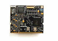
Manufacturer Part Number
ADSP-3PARCBF548M01
Description
MODULE BOARD BF548
Manufacturer
Analog Devices Inc
Series
Blackfin®r
Specifications of ADSP-3PARCBF548M01
Module/board Type
Processor Module
For Use With/related Products
ADSP-BF548
Lead Free Status / RoHS Status
Lead free / RoHS Compliant


ADSP-BF542/ADSP-BF544/ADSP-BF547/ADSP-BF548/ADSP-BF549
TABLE OF CONTENTS
General Description ................................................. 3
REVISION HISTORY
2/10—Rev. B to Rev. C
Added V
Added I
Absolute Maximum Ratings .................................................... 40
Added
Revised all timing diagrams for clarity/consistency in
Specifications ........................................................ 42
Updated specifications (reference PCN 09_0173) in the
and Reset Timing
startup/reset
Added t
Clock)
Low Power Architecture ......................................... 4
System Integration ................................................ 4
Blackfin Processor Peripherals ................................. 4
Blackfin Processor Core .......................................... 4
Memory Architecture ............................................ 6
DMA Controllers ................................................ 10
Real-Time Clock ................................................. 11
Watchdog Timer ................................................ 12
Timers ............................................................. 12
Up/Down Counter and Thumbwheel Interface .......... 12
Serial Ports (SPORTs) .......................................... 12
Serial Peripheral Interface (SPI) Ports ...................... 13
UART Ports (UARTs) .......................................... 13
Controller Area Network (CAN) ............................ 13
TWI Controller Interface ...................................... 14
Ports ................................................................ 14
Pixel Compositor (PIXC) ...................................... 14
Enhanced Parallel Peripheral Interface (EPPI) ........... 14
USB On-the-Go Dual-Role Device Controller ............ 15
ATA/ATAPI-6 Interface ....................................... 15
Keypad Interface ................................................. 15
Secure Digital (SD)/SDIO Controller ....................... 16
Code Security .................................................... 16
Media Transceiver MAC Layer (MXVR) .................. 16
Dynamic Power Management ................................ 16
Voltage Regulation .............................................. 18
Clock Signals ..................................................... 18
Table 23 (Total Current Pin
.................................................................. 61
SUDTE
OH
IHTWI
/I
OL
timing.................................................. 42
and t
and V
per pin group data to
section to accurately describe processor cold-
SUDRE
ILTWI
data to
data to
Table 41 (Serial Ports—External
Operating Conditions ...... 34
Groups)
........................ 40
Rev. C | Page 2 of 100 | February 2010
Timing
Clock
Pin Descriptions .................................................... 25
Specifications ........................................................ 34
400-Ball CSP_BGA Package ...................................... 92
Outline Dimensions ................................................ 98
Automotive Products .............................................. 99
Ordering Guide ................................................... 100
Added t
Clock)
Added
Frame
State)
To view product/process change notifications (PCNs) related to
this data sheet revision, please visit the processor's product page
on the
Booting Modes ................................................... 19
Instruction Set Description .................................... 22
Development Tools .............................................. 23
Designing an Emulator-Compatible Processor Board ... 23
MXVR Board Layout Guidelines ............................. 23
Related Documents .............................................. 24
Lockbox Secure Technology Disclaimer .................... 24
Operating Conditions ........................................... 34
Electrical Characteristics ....................................... 36
Absolute Maximum Ratings ................................... 40
ESD Sensitivity ................................................... 41
Package Information ............................................ 41
Timing Specifications ........................................... 42
Output Drive Currents ......................................... 86
Test Conditions .................................................. 88
Capacitive Loading .............................................. 88
Typical Rise and Fall Times ................................... 89
Thermal Characteristics ........................................ 91
Surface-Mount Design .......................................... 98
EZ-KIT Lite Evaluation Board ............................. 23
............................................................................................ 62
www.analog.com
Sync) and
Figure 34 (Serial Port Start-Up with External Clock and
..................................................................61
SCLKIW
and t
Figure 36 (Serial Ports—Enable and Three-
SCLK
data to
website and use the View PCN link.
Table 42 (Serial Ports—Internal
Related parts for ADSP-3PARCBF548M01
Image
Part Number
Description
Manufacturer
Datasheet
Request
R

Part Number:
Description:
±1.7g Dual-Axis IMEMS Accelerometer Evaluation Board
Manufacturer:
Analog Devices Inc
Datasheet:

Part Number:
Description:
Inertial Sensor Evaluation System
Manufacturer:
Analog Devices Inc
Datasheet:
Part Number:
Description:
Manufacturer:
Analog Devices Inc
Datasheet:
Part Number:
Description:
Manufacturer:
Analog Devices Inc
Datasheet:
Part Number:
Description:
Manufacturer:
Analog Devices Inc
Datasheet:
Part Number:
Description:
Manufacturer:
Analog Devices Inc
Datasheet:
Part Number:
Description:
Manufacturer:
Analog Devices Inc
Datasheet:
Part Number:
Description:
Manufacturer:
Analog Devices Inc
Datasheet:
Part Number:
Description:
Manufacturer:
Analog Devices Inc
Datasheet:
Part Number:
Description:
Manufacturer:
Analog Devices Inc
Datasheet:
Part Number:
Description:
Manufacturer:
Analog Devices Inc
Datasheet:
Part Number:
Description:
Manufacturer:
Analog Devices Inc
Datasheet:
Part Number:
Description:
Manufacturer:
Analog Devices Inc
Datasheet: