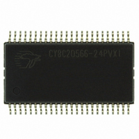
CY8C20566-24PVXI Cypress Semiconductor Corp, CY8C20566-24PVXI Datasheet - Page 25

CY8C20566-24PVXI
Manufacturer Part Number
CY8C20566-24PVXI
Description
IC MCU 32K FLASH 2K SRAM 48SSOP
Manufacturer
Cypress Semiconductor Corp
Series
CapSense® Controllersr
Specifications of CY8C20566-24PVXI
Applications
Capacitive Sensing
Core Processor
M8C
Program Memory Type
FLASH (32 kB)
Controller Series
CY8C20xx6
Ram Size
2K x 8
Interface
I²C, SPI
Number Of I /o
36
Voltage - Supply
1.71 V ~ 5.5 V
Operating Temperature
-40°C ~ 85°C
Mounting Type
Surface Mount
Package / Case
48-SSOP
Operating Temperature (min)
-40C
Operating Temperature (max)
85C
Technology
CMOS
Processing Unit
Microprocessor
Operating Supply Voltage (min)
1.71V
Operating Supply Voltage (typ)
1.8/2.5/3.3/5V
Operating Supply Voltage (max)
5.5V
Package Type
SSOP
Screening Level
Industrial
Pin Count
48
Mounting
Surface Mount
Rad Hardened
No
Processor Series
CY8C20x66
Core
M8C
Data Bus Width
8 bit
Program Memory Size
32 KB
Data Ram Size
2 KB
Interface Type
I2C, SPI, USB
Maximum Clock Frequency
24 MHz
Number Of Programmable I/os
36
Number Of Timers
3
Maximum Operating Temperature
+ 85 C
Mounting Style
SMD/SMT
Development Tools By Supplier
CY3280-20X66
Minimum Operating Temperature
- 40 C
Lead Free Status / RoHS Status
Lead free / RoHS Compliant
For Use With
770-1000 - ISP 4PORT FOR CYPRESS PSOC MCU
Lead Free Status / Rohs Status
Details
Other names
428-2947
Available stocks
Company
Part Number
Manufacturer
Quantity
Price
Company:
Part Number:
CY8C20566-24PVXI
Manufacturer:
CYPRESS
Quantity:
47
AC SPI Specifications
The following table lists guaranteed maximum and minimum specifications for the entire voltage and temperature ranges.
Table 31. AC SPI Specifications
AC I
The following table lists guaranteed maximum and minimum specifications for the entire voltage and temperature ranges.
Table 32. AC Characteristics of the I
Document Number: 001-12696 Rev. *D
Note
F
F
T
F
T
T
T
T
T
T
T
T
T
10. A Fast-Mode I2C-bus device can be used in a Standard Mode I2C-bus system, but the requirement t
SPIM
SPIS
SS
SCLI2C
HDSTAI2C
LOWI2C
HIGHI2C
SUSTAI2C
HDDATI2C
SUDATI2C
SUSTOI2C
BUFI2C
SPI2C
Symbol
Symbol
SDA
if the device does not stretch the LOW period of the SCL signal. If such device does stretch the LOW period of the SCL signal, it must output the next data bit to the
SDA line t
SCL
2
C Specifications
rmax
Maximum Input Clock Frequency Selection,
Master 2.4V<Vdd<5.5V
Maximum Input Clock Frequency Selection,
Master
Maximum Input Clock Frequency Selection,
Slave 2.4<Vdd<5.5V
Maximum Input Clock Frequency Selection,
Slave 1.71V<Vdd<2.4V
Width of SS_ Negated Between Transmissions
SCL Clock Frequency
Hold Time (repeated) START Condition. After this period, the first clock pulse is
generated.
LOW Period of the SCL Clock
HIGH Period of the SCL Clock
Setup Time for a Repeated START Condition
Data Hold Time
Data Setup Time
Setup Time for STOP Condition
Bus Free Time Between a STOP and START Condition
Pulse Width of spikes are suppressed by the input filter.
S
+ t
T
SU;DAT
HDSTAI2C
T
(21)
LOWI2C
1.71V<Vdd<2.4V
= 1000 + 250 = 1250 ns (according to the Standard-Mode I2C-bus specification) before the SCL line is released.
T
Figure 13. Definition for Timing for Fast/Standard Mode on the I
HDDATI2C
Description
T
T
HIGHI2C
2
C SDA and SCL Pins
SUDATI2C
Description
T
SUSTAI2C
Output clock frequency is half
of input clock rate.
Output clock frequency is half
of input clock rate
Sr
Conditions
T
HDSTAI2C
SU;DAT
CY8C20x36/46/66, CY8C20396
≥ 250 ns must then be met. This automatically be the case
T
SUSTOI2C
T
SPI2C
Standard Mode Fast Mode
Min
250
4.0
4.7
4.0
4.7
4.7
4.0
0
0
–
2
Min
C Bus
50
–
–
Max
100
P
–
–
–
–
–
–
–
–
–
T
Typ
BUFI2C
–
–
–
100
Min
0.6
1.3
0.6
0.6
0.6
1.3
0]
0
0
0
[1
Max
S
Page 25 of 34
12
12
Max
400
6
6
–
50
–
–
–
–
–
–
–
–
Units
Units
MHz
MHz
MHz
MHz
kHz
μs
μs
μs
μs
μs
ns
μs
μs
ns
ns
[+] Feedback


