CY7C63613-SC Cypress Semiconductor Corp, CY7C63613-SC Datasheet - Page 4
CY7C63613-SC
Manufacturer Part Number
CY7C63613-SC
Description
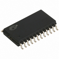
IC MCU 8K USB LS MCU 24-SOIC
Manufacturer
Cypress Semiconductor Corp
Series
M8™r
Datasheet
1.CY7C63613-SC.pdf
(30 pages)
Specifications of CY7C63613-SC
Applications
USB Microcontroller
Core Processor
M8B
Program Memory Type
OTP (8 kB)
Controller Series
CY7C636xx
Ram Size
256 x 8
Interface
PS2, USB
Number Of I /o
16
Voltage - Supply
4 V ~ 5.5 V
Operating Temperature
0°C ~ 70°C
Mounting Type
Surface Mount
Package / Case
24-SOIC (7.5mm Width)
Lead Free Status / RoHS Status
Contains lead / RoHS non-compliant
Other names
428-1321
Available stocks
Company
Part Number
Manufacturer
Quantity
Price
Company:

Part Number:
CY7C63613-SC
Manufacturer:
CYP
Quantity:
5 510
Part Number:
CY7C63613-SC
Manufacturer:
CYPRESS/赛普拉斯
Quantity:
20 000


FOR
FOR
PRELIMINARY
CY7C63612/13
LIST OF FIGURES
Figure 6-1. Program Memory Space with Interrupt Vector Table ......................................................... 11
Figure 7-1. Clock Oscillator On-chip Circuit .......................................................................................... 14
Figure 8-1. Watch Dog Reset (WDR) ................................................................................................... 15
Figure 9-1. Block Diagram of a GPIO Line ........................................................................................... 15
Figure 9-2. Port 0 Data 0x00h (read/write) ........................................................................................... 16
Figure 9-3. Port 1 Data 0x01h (read/write) ........................................................................................... 16
Figure 9-4. Port 2 Data 0x02h (read/write) ........................................................................................... 16
Figure 9-5. Port 3 Data 0x03h (read/write) ........................................................................................... 16
Figure 9-6. DAC Port Data 0x30h (read/write) ...................................................................................... 16
Figure 9-7. Port 0 Interrupt Enable 0x04h (write only) .......................................................................... 16
Figure 9-8. Port 1 Interrupt Enable 0x05h (write only) .......................................................................... 16
Figure 9-9. Port 2 Interrupt Enable 0x06h (write only) .......................................................................... 16
Figure 9-10. Port 3 Interrupt Enable 0x07h (write only) ........................................................................ 16
Figure 9-11. GPIO Configuration Register 0x08h (write only) .............................................................. 17
Figure 10-1. USB Status and Control Register 0x1Fh .......................................................................... 18
Figure 11-1. USB Device Address Register 0x10h (read/write) ........................................................... 19
Figure 11-2. USB Device EPA0 Mode Register 0x12h (read/write) ..................................................... 19
Figure 11-3. USB Device Endpoint Mode Registers 0x14h, 0x16h (read/write) ................................... 19
Figure 11-4. USB Device Counter Registers 0x11h, 0x13h, 0x15h (read/write) .................................. 20
Figure 12-1. Timer Register 0x24h (read only) ..................................................................................... 20
Figure 12-2. Timer Register 0x25h (read only) ..................................................................................... 20
Figure 12-3. Timer Block Diagram ........................................................................................................ 20
Figure 13-1. Processor Status and Control Register 0xFFh ................................................................. 21
Figure 14-1. Global Interrupt Enable Register 0x20h (read/write) ........................................................ 21
Figure 14-2. USB End Point Interrupt Enable Register 0x21h (read/write) .......................................... 22
Figure 18-1. Clock Timing ..................................................................................................................... 28
Figure 18-2. USB Data Signal Timing ................................................................................................... 29
Figure 18-3. Receiver Jitter Tolerance ................................................................................................. 29
Figure 18-4. Differential to EOP Transition Skew and EOP Width ....................................................... 29
Figure 18-5. Differential Data Jitter ....................................................................................................... 30
LIST OF TABLES
Table 6-1. I/O Register Summary ........................................................................................................ 13
Table 14-1. Interrupt Vector Assignments ........................................................................................... 22
Table 15-1. USB Register Mode Encoding .......................................................................................... 23
Table 15-2. Decode table for Table 15-3 : “Details of Modes for Differing Traffic Conditions” .............. 24
Table 15-3. Details of Modes for Differing Traffic Conditions .............................................................. 25
4
Related parts for CY7C63613-SC
Image
Part Number
Description
Manufacturer
Datasheet
Request
R

Part Number:
Description:
Manufacturer:
Cypress Semiconductor Corp
Datasheet:
Part Number:
Description:
Manufacturer:
Cypress Semiconductor Corp
Datasheet:
Part Number:
Description:
Manufacturer:
Cypress Semiconductor Corp
Datasheet:
Part Number:
Description:
Manufacturer:
Cypress Semiconductor Corp
Datasheet:
Part Number:
Description:
Manufacturer:
Cypress Semiconductor Corp
Datasheet: