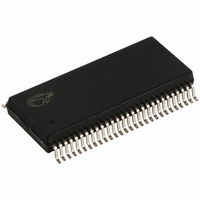
CY7C66113-PVC Cypress Semiconductor Corp, CY7C66113-PVC Datasheet - Page 17

CY7C66113-PVC
Manufacturer Part Number
CY7C66113-PVC
Description
IC MCU 8K USB HUB 4 PORT 56TSSOP
Manufacturer
Cypress Semiconductor Corp
Specifications of CY7C66113-PVC
Applications
USB Hub/Microcontroller
Core Processor
M8
Program Memory Type
OTP (8 kB)
Controller Series
USB Hub
Ram Size
256 x 8
Interface
I²C, USB, HAPI
Number Of I /o
31
Voltage - Supply
4 V ~ 5.5 V
Operating Temperature
0°C ~ 70°C
Mounting Type
Surface Mount
Package / Case
56-SSOP
Operating Temperature (max)
70C
Operating Temperature (min)
0C
Operating Temperature Classification
Commercial
Mounting
Surface Mount
Pin Count
56
Lead Free Status / RoHS Status
Contains lead / RoHS non-compliant
For Use With
CY3649 - PROGRAMMER HI-LO USB M8428-1339 - KIT LOW SPEED PERSONALITY BOARD
Lead Free Status / RoHS Status
Not Compliant, Contains lead / RoHS non-compliant
Other names
428-1330
Available stocks
Company
Part Number
Manufacturer
Quantity
Price
Company:
Part Number:
CY7C66113-PVC
Manufacturer:
CY
Quantity:
10
If the 1.024-ms timer interrupt service routine does not get executed for t
occur. A Watch Dog Timer Reset lasts for 2 ms after which the microcontroller begins execution at ROM address 0x0000. The
USB transmitter is disabled by a Watch Dog Reset because the USB Device Address Registers are cleared. Otherwise, the USB
Controller would respond to all address 0 transactions.
8.0
There are up to 31 GPIO pins (P0[7:0], P1[7:0], P2[7:0], and P3[6:0]) for the hardware interface. The number of GPIO pins
changes based on the package type of the chip. Each port can be configured as inputs with internal pull-ups, open drain outputs,
or traditional CMOS outputs. Ports 0 to 2 are considered low current drive with typical current sink capability of 7 mA. Port 3 offers
higher current drive with a typical current sink capability of 12 mA. The data for each GPIO port is accessible through the data
registers.
Special care should be exercised with any unused GPIO data bits. An unused GPIO data bit, either a pin on the chip or a port bit
that is not bonded on a particular package, must not be left floating when the device enters the suspend state. If a GPIO data bit
is left floating, the leakage current caused by the floating bit may violate the suspend current limitation specified by the USB
Specifications. If a ‘1’ is written to the unused data bit and the port is configured with open drain outputs, the unused data bit will
P0[7]
P1[7]
P2[7]
P3[7]
General-Purpose I/O Ports
P0[6]
P1[6]
P2[6]
P3[6]
Interrupt
Enable
Interrupt
Controller
Port Write
OE
Port Read
Reg_Bit
Internal
Data Bus
STRB
GPIO
CFG
P0[5]
P1[5]
P2[5]
P3[5]
PRELIMINARY
Figure 8-1. Block Diagram of a GPIO Pin
Figure 8-2. Port 0 Data 0x00 (read/write)
Figure 8-3. Port 1 Data 0x01 (read/write)
Figure 8-4. Port 2 Data 0x02 (read/write)
Figure 8-5. Port 3 Data 0x03 (read/write)
Data
In
Latch
Data
Interrupt
Latch
Data
Out
Latch
P0[4]
P1[4]
P2[4]
P3[4]
mode
2-bits
17
P0[3]
P1[3]
P2[3]
P3[3]
Q3*
*Port 0,1,2: Low I
Q1
14 K
Port 3: High I
WATCH
V
CC
(8 ms minimum) a Watch Dog Timer Reset will
Q2
P0[2]
P1[2]
P2[2]
P3[2]
sink
sink
GPIO
Pad
CY7C66011/12/13
CY7C66111/12/13
P0[1]
P1[1]
P2[1]
P3[1]
P0[0]
P1[0]
P2[0]
P3[0]


