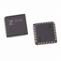
Z85C3008VSG Zilog, Z85C3008VSG Datasheet - Page 20

Z85C3008VSG
Manufacturer Part Number
Z85C3008VSG
Description
IC 8MHZ Z8500 CMOS SCC 44-PLCC
Manufacturer
Zilog
Series
SCCr
Specifications of Z85C3008VSG
Processor Type
Z80
Features
Error Detection and Multiprotocol Support
Speed
8MHz
Voltage
5V
Mounting Type
Surface Mount
Package / Case
44-LCC (J-Lead)
Maximum Operating Temperature
+ 70 C
Minimum Operating Temperature
0 C
Mounting Style
SMD/SMT
Cpu Speed
8MHz
Digital Ic Case Style
LCC
No. Of Pins
44
Supply Voltage Range
5V
Operating Temperature Range
0°C To +70°C
Svhc
No SVHC (18-Jun-2010)
Base Number
85
Rohs Compliant
Yes
Clock Frequency
8MHz
Lead Free Status / RoHS Status
Lead free / RoHS Compliant
Other names
269-3932
Z85C3008VSG
Z85C3008VSG
Available stocks
Company
Part Number
Manufacturer
Quantity
Price
Company:
Part Number:
Z85C3008VSG
Manufacturer:
Zilog
Quantity:
800
Company:
Part Number:
Z85C3008VSG
Manufacturer:
MAX
Quantity:
74
PS011705-0608
Table 2. SCC Write Register Functions (continued)
Following three methods move data, status, and control information in and out of
the SCC:
Polling
When polling, all interrupts are disabled. Three status registers in the SCC are automati-
cally updated when any function is performed. For example, End-Of-Frame in SDLC
mode sets a bit in one of these status registers. The purpose of polling is for the CPU to
periodically read a status register until the register contents indicate the need for data to be
transferred. Only one register is read, and depending on its contents, the CPU either writes
data, reads data, or continues. Two bits in the register indicate the need for data transfer.
An alternative is a poll of the Interrupt Pending register to determine the source of an
interrupt. The status for both channels resides in one register.
Interrupts
The SCC’s interrupt structure supports vectored and nested interrupts. Nested interrupts
are supported with the interrupt acknowledge feature (INTACK pin) of the SCC.
This allows the CPU to recognize the occurrence of an interrupt, and re-enable higher pri-
ority interrupts. Because an INTACK cycle releases the INT pin from the active state, a
higher priority SCC interrupt or another higher priority device can interrupt the CPU.
When an SCC responds to an Interrupt Acknowledge signal (INTACK) from the CPU, an
interrupt vector can be placed on the data bus. This vector is written in WR2 and can be
read in RR2A or RR2B. To speed interrupt response time, the SCC can modify three bits
in this vector to indicate status. If the vector is read in Channel A, status is never included.
If the vector is read in Channel B, status is always included.
Each of the six sources of interrupts in the SCC (Transmit, Receive, and External/Status
interrupts in both channels) has three bits associated with the interrupt source.
Register
WR11
WR12
WR13
WR14
WR15
•
•
•
Polling
Interrupts
CPU/DMA Block Transfer
under CPU or DMA control.
(vectored and non-vectored)
Function
Clock mode control
Lower byte of Baud Rate Generator time constant
Upper byte of Baud Rate Generator time constant
Miscellaneous control bits
External/Status interrupt control
— The BLOCK TRANSFER mode can be implemented
CMOS SCC Serial Communications Controller
Product Specification
Functional Description
16


