MPC5200CVR400B Freescale Semiconductor, MPC5200CVR400B Datasheet - Page 19
MPC5200CVR400B
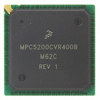
Manufacturer Part Number
MPC5200CVR400B
Description
IC MPU 32BIT 400MHZ 272-PBGA
Manufacturer
Freescale Semiconductor
Specifications of MPC5200CVR400B
Processor Type
MPC52xx PowerPC 32-Bit
Speed
400MHz
Voltage
1.5V
Mounting Type
Surface Mount
Package / Case
272-PBGA
Processor Series
MPC52xx
Core
e300
Development Tools By Supplier
MEDIA5200KIT1E
Maximum Clock Frequency
400 MHz
Maximum Operating Temperature
+ 105 C
Mounting Style
SMD/SMT
I/o Voltage
2.5 V, 3.3 V
Minimum Operating Temperature
- 40 C
Core Size
32 Bit
No. Of I/o's
56
Ram Memory Size
16KB
Cpu Speed
400MHz
No. Of Timers
8
Embedded Interface Type
CAN, I2C, SCI, SPI
No. Of Pwm Channels
8
Digital Ic Case Style
TEPBGA
Rohs Compliant
Yes
Lead Free Status / RoHS Status
Lead free / RoHS Compliant
Features
-
Lead Free Status / Rohs Status
Lead free / RoHS Compliant
Available stocks
Company
Part Number
Manufacturer
Quantity
Price
Company:

Part Number:
MPC5200CVR400B
Manufacturer:
Marvell
Quantity:
1 001
Company:
Part Number:
MPC5200CVR400B
Manufacturer:
FREESCAL
Quantity:
200
Company:
Part Number:
MPC5200CVR400B
Manufacturer:
Freescale Semiconductor
Quantity:
10 000
Part Number:
MPC5200CVR400B
Manufacturer:
FREESCALE
Quantity:
20 000
Company:
Part Number:
MPC5200CVR400BM62C
Manufacturer:
FRRESCAL..
Quantity:
2 831


1.3.6.3
The SDRAM Memory Controller uses a 1/4 period delayed MDQS strobe to capture the MDQ data. The 1/4 period delay value
is calculated automatically by hardware.
Freescale Semiconductor
data
t
data
mem_clk
MBA (Bank Selects)
Sym
t
t
valid
hold
DQM (Data Mask)
setup
hold
Control Signals
MA (Address)
NOTE: Control Signals are composed of RAS, CAS, MEM_WE, MEM_CS, MEM_CS1 and CLK_EN
MDQ (Data)
MEM_CLK
Memory Interface Timing-DDR SDRAM Read Command
valid after rising edge of MEM_CLK
hold after rising edge of MEM_CLK
Control Signals, Address and MBA
Control Signals, Address and MBA
Setup time relative to MDQS
Hold time relative to MDQS
Figure 6. Timing Diagram—Standard SDRAM Memory Write Timing
MEM_CLK period
Description
t
t
t
valid
valid
valid
Table 20. DDR SDRAM Memory Read Timing
Active
Row
t
t
t
data
hold
hold
hold
DM
valid
MPC5200B Data Sheet, Rev. 4
valid
NOP
WRITE
Column
t
mem_clk
Min
7.5
2.6
—
—
DM
data
× 0.5
NOP
hold
hold
NOP
t
mem_clk
NOP
Max
0.4
× 0.5 + 0.4
—
—
—
NOP
Units
ns
ns
ns
ns
ns
NOP
SpecID
A5.16
A5.17
A5.18
A5.19
A5.15
19
Related parts for MPC5200CVR400B
Image
Part Number
Description
Manufacturer
Datasheet
Request
R

Part Number:
Description:
Manufacturer:
Freescale Semiconductor, Inc
Datasheet:
Part Number:
Description:
Manufacturer:
Freescale Semiconductor, Inc
Datasheet:
Part Number:
Description:
Manufacturer:
Freescale Semiconductor, Inc
Datasheet:
Part Number:
Description:
Manufacturer:
Freescale Semiconductor, Inc
Datasheet:
Part Number:
Description:
Manufacturer:
Freescale Semiconductor, Inc
Datasheet:
Part Number:
Description:
Manufacturer:
Freescale Semiconductor, Inc
Datasheet:
Part Number:
Description:
Manufacturer:
Freescale Semiconductor, Inc
Datasheet:
Part Number:
Description:
Manufacturer:
Freescale Semiconductor, Inc
Datasheet:
Part Number:
Description:
Manufacturer:
Freescale Semiconductor, Inc
Datasheet:
Part Number:
Description:
Manufacturer:
Freescale Semiconductor, Inc
Datasheet:
Part Number:
Description:
Manufacturer:
Freescale Semiconductor, Inc
Datasheet:
Part Number:
Description:
Manufacturer:
Freescale Semiconductor, Inc
Datasheet:
Part Number:
Description:
Manufacturer:
Freescale Semiconductor, Inc
Datasheet:
Part Number:
Description:
Manufacturer:
Freescale Semiconductor, Inc
Datasheet:
Part Number:
Description:
Manufacturer:
Freescale Semiconductor, Inc
Datasheet: