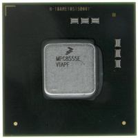
MPC8555EVTAPF Freescale Semiconductor, MPC8555EVTAPF Datasheet - Page 43

MPC8555EVTAPF
Manufacturer Part Number
MPC8555EVTAPF
Description
IC MPU POWERQUICC III 783-FCPBGA
Manufacturer
Freescale Semiconductor
Datasheet
1.MPC8555ECVTALF.pdf
(88 pages)
Specifications of MPC8555EVTAPF
Processor Type
MPC85xx PowerQUICC III 32-Bit
Speed
833MHz
Voltage
1.2V
Mounting Type
Surface Mount
Package / Case
783-FCPBGA
For Use With
MPC8555CDS - BOARD EVALUATION CDS FOR 8555CWH-PPC-8555N-VX - BOARD EVAL QUICCSTART MPC8555CWH-PPC-8540N-VE - KIT EVAL SYSTEM MPC8540CWH-PPC-8555N-VE - EVALUATION SYSTEM QUICC MPC8555E
Lead Free Status / RoHS Status
Not applicable / RoHS Compliant
Features
-
Available stocks
Company
Part Number
Manufacturer
Quantity
Price
Company:
Part Number:
MPC8555EVTAPF
Manufacturer:
Freescale Semiconductor
Quantity:
10 000
Part Number:
MPC8555EVTAPF
Manufacturer:
FREESCALE
Quantity:
20 000
10 CPM
This section describes the DC and AC electrical specifications for the CPM of the MPC8555E.
10.1
Table 32
10.2
Table 33
Freescale Semiconductor
Input high voltage
Input low voltage
Output high voltage
Output low voltage
Output high voltage
Output low voltage
Note:
1. This specification applies to the following pins: PA[0–31], PB[4–31], PC[0–31], and PD[4–31].
2. V
FCC inputs—internal clock (NMSI) input setup time
FCC inputs—internal clock (NMSI) hold time
FCC inputs—external clock (NMSI) input setup time
FCC inputs—external clock (NMSI) hold time
SCC/SMC/SPI inputs—internal clock (NMSI) input setup time
SCC/SMC/SPI inputs—internal clock (NMSI) input hold time
SCC/SMC/SPI inputs—external clock (NMSI) input setup time
SCC/SMC/SPI inputs—external clock (NMSI) input hold time
TDM inputs/SI—input setup time
IL
(max) for the IIC interface is 0.8 V rather than the 1.5 V specified in the IIC standard
MPC8555E PowerQUICC™ III Integrated Communications Processor Hardware Specification, Rev. 4.2
provides the DC electrical characteristics for the CPM.
and
CPM DC Electrical Characteristics
CPM AC Timing Specifications
Characteristic
Table 34
It is recommended that the rise/fall time on CPM input pins should not
exceed 5 ns. This should be enforced especially on clock signals. Rise time
refers to signal transitions from 10% to 90% of VCC; fall time refers to
transitions from 90% to 10% of VCC.
provide the CPM input and output AC timing specifications, respectively.
Table 33. CPM Input AC Timing Specifications
Characteristic
Table 32. CPM DC Electrical Characteristics
NOTE: Rise/Fall Time on CPM Input Pins
Symbol
V
V
V
V
V
V
OH
OH
OL
OL
IH
IL
I
I
OH
OH
I
I
OL
OL
Condition
= –8.0 mA
= –2.0 mA
= 3.2 mA
= 8.0 mA
GND
Min
2.0
2.4
2.4
—
—
Symbol
1
t
FEIXKH
t
t
t
t
t
t
t
t
NEIVKH
NEIXKH
FEIVKH
TDIVKH
FIIVKH
FIIXKH
NIIVKH
NIIXKH
3.465
b
Max
2
0.8
0.5
0.4
—
—
Min
2.5
6
0
2
6
0
4
2
4
Unit
3
V
V
V
V
V
V
Notes
Unit
ns
ns
ns
ns
ns
ns
ns
ns
ns
1, 2
1
1
1
1
1
CPM
43


