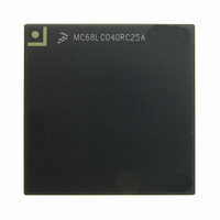
MC68LC040RC25A Freescale Semiconductor, MC68LC040RC25A Datasheet - Page 164

MC68LC040RC25A
Manufacturer Part Number
MC68LC040RC25A
Description
IC MPU 32BIT 25MHZ 179-PGA
Manufacturer
Freescale Semiconductor
Datasheet
1.MC68EC040FE33A.pdf
(442 pages)
Specifications of MC68LC040RC25A
Processor Type
M680x0 32-Bit
Speed
25MHz
Voltage
5V
Mounting Type
Surface Mount
Package / Case
179-PGA
Lead Free Status / RoHS Status
Lead free / RoHS Compliant
Features
-
Available stocks
Company
Part Number
Manufacturer
Quantity
Price
Company:
Part Number:
MC68LC040RC25A
Manufacturer:
MOT
Quantity:
6 100
Company:
Part Number:
MC68LC040RC25A
Manufacturer:
Freescale Semiconductor
Quantity:
135
- Current page: 164 of 442
- Download datasheet (4Mb)
Clock 2 (C2)
7.4.4 Line Write Transfers
The processor uses line write bus cycles to access a 16-byte operand for a MOVE16
instruction and to support cache line pushes. Both burst and burst-inhibited transfers are
supported. Figures 7-16 and 7-17 illustrate a flowchart and functional timing diagram for a
line write bus cycle.
7-22
During the first half of the clock after C1, the processor negates TS and drives the
appropriate bytes of the data bus with the data to be written. All other bytes are driven
with undefined values. The selected device uses R/W, SIZ1, SIZ0, A1, A0, and CIOUT
to latch only the required information on the data bus. With the exception of R/W and
CIOUT, these signals also select any or all of the bytes (D31–D24, D23–D16, D15–D8,
and D7–D0). If the first clock after C1 is not a wait state, then the selected peripheral
device asserts the TA signal.
At the end of the first clock cycle after C1, the processor samples the level of T A,
terminating the bus cycle if TA is asserted. If TA is not recognized asserted at the end of
the clock cycle, the processor ignores the data and inserts a wait state instead of
terminating the transfer. The processor continues to sample TA on successive rising
edges of BCLK until TA is recognized asserted. The data bus then three-states and the
bus cycle ends.
When the processor recognizes TA at the clock edge and terminates the bus cycle, TIP
remains asserted if the processor is ready to begin another bus cycle. Otherwise, the
processor negates TIP during the first half of the next clock. The processor also three-
states the data bus during the first half of the next clock following termination of the
write transfer.
Freescale Semiconductor, Inc.
For More Information On This Product,
M68040 USER’S MANUAL
Go to: www.freescale.com
MOTOROLA
Related parts for MC68LC040RC25A
Image
Part Number
Description
Manufacturer
Datasheet
Request
R
Part Number:
Description:
Manufacturer:
Freescale Semiconductor, Inc
Datasheet:
Part Number:
Description:
Manufacturer:
Freescale Semiconductor, Inc
Datasheet:
Part Number:
Description:
Manufacturer:
Freescale Semiconductor, Inc
Datasheet:
Part Number:
Description:
Manufacturer:
Freescale Semiconductor, Inc
Datasheet:
Part Number:
Description:
Manufacturer:
Freescale Semiconductor, Inc
Datasheet:
Part Number:
Description:
Manufacturer:
Freescale Semiconductor, Inc
Datasheet:
Part Number:
Description:
Manufacturer:
Freescale Semiconductor, Inc
Datasheet:
Part Number:
Description:
Manufacturer:
Freescale Semiconductor, Inc
Datasheet:
Part Number:
Description:
Manufacturer:
Freescale Semiconductor, Inc
Datasheet:
Part Number:
Description:
Manufacturer:
Freescale Semiconductor, Inc
Datasheet:
Part Number:
Description:
Manufacturer:
Freescale Semiconductor, Inc
Datasheet:
Part Number:
Description:
Manufacturer:
Freescale Semiconductor, Inc
Datasheet:
Part Number:
Description:
Manufacturer:
Freescale Semiconductor, Inc
Datasheet:
Part Number:
Description:
Manufacturer:
Freescale Semiconductor, Inc
Datasheet:
Part Number:
Description:
Manufacturer:
Freescale Semiconductor, Inc
Datasheet:


