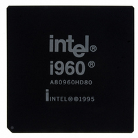
A80960HD80SL2GK Intel, A80960HD80SL2GK Datasheet - Page 16

A80960HD80SL2GK
Manufacturer Part Number
A80960HD80SL2GK
Description
IC I960HD 3.3V 80MHZ 168CPGA
Manufacturer
Intel
Datasheet
1.UG80960HD6616SL2GN.pdf
(104 pages)
Specifications of A80960HD80SL2GK
Rohs Status
RoHS non-compliant
Processor Type
i960
Features
HD suffix, 32-Bit, 40MHz Bus
Speed
80MHz
Voltage
3.3V
Mounting Type
Surface Mount
Package / Case
168-CPGA
Other names
815177
80960HA/HD/HT
16
Table 7.
80960Hx Processor Family Pin Descriptions (Sheet 1 of 4)
DP3:0
PCHK
BE3:0
Name
A31:2
D31:0
W/R
D/C
Type
H(Q)
B(Q)
H(Z)
R(Z)
H(Z)
R(Z)
H(Z)
R(Z)
H(Z)
H(Z)
H(Z)
B(Z)
S(L)
B(Z)
S(L)
B(Z)
R(1)
B(Z)
R(1)
B(Z)
R(0)
B(Z)
R(0)
I/O
I/O
O
O
O
O
O
ADDRESS BUS carries the upper 30 bits of the physical address. A31 is the most
significant address bit and A2 is the least significant. During a bus access, A31:2
identify all external addresses to word (4-byte) boundaries. The byte enable
signals indicate the selected byte in each word. During burst accesses, A3 and
A2 increment to indicate successive addresses.
DATA BUS carries 32, 16, or 8-bit data quantities depending on bus width
configuration. The least significant bit of the data is carried on D0 and the most
significant on D31. The lower eight data lines (D7:0) are used when the bus is
configured for 8-bit data. When configured for 16-bit data, D15:0 are used.
DATA PARITY carries parity information for the data bus. Each parity bit is
assigned a group of eight data bus pins as follows:
Parity information is generated for a processor write cycle and is checked for a
processor read cycle. Parity checking and polarity are programmable. Parity
generation/checking is only performed for the size of the data accessed.
PARITY CHECK indicates the result of a parity check operation. An asserted
PCHK indicates that the previous bus read access resulted in a parity check error.
BYTE ENABLES select which of the four bytes addressed by A31:2 are active
during a bus access. Byte enable encoding is dependent on the bus width of the
memory region accessed:
32-bit bus:
16-bit bus:
8-bit bus:
WRITE/READ is low for read accesses and high for write accesses.
W/R becomes valid during the address phase of a bus cycle and remains valid
until the end of the cycle for non-pipelined accesses. For pipelined accesses, W/
R changes state when the next address is presented.
0= Read
1= Write
DATA/CODE indicates that a bus access is a data access or an instruction
access. D/C has the same timing as W/R.
0 = Code
1 = Data
DP3 generates/checks parity for D31:24
DP2 generates/checks parity for D23:16
DP1 generates/checks parity for D15:8
DP0 generates/checks parity for D7:0
BE3 enables D31:24
BE2 enables D23:16
BE1 enables D15:8
BE0 enables D7:0
BE3 becomes Byte High Enable (enables D15:8)
BE2 is not used (state is undefined)
BE1 becomes Address Bit 1 (A1)
BE0 becomes Byte Low Enable (enables D7:0)
BE3 is not used (state is undefined)
BE2 is not used (state is undefined)
BE1 Address Bit 1 (A1)
BE0 Address Bit 0 (A0)
Description
Datasheet


