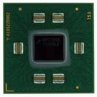
MPC755CPX400LE Freescale Semiconductor, MPC755CPX400LE Datasheet - Page 16

MPC755CPX400LE
Manufacturer Part Number
MPC755CPX400LE
Description
IC MPU PPC 400MHZ 360-FCPBGA
Manufacturer
Freescale Semiconductor
Datasheet
1.MPC755BPX300LE.pdf
(56 pages)
Specifications of MPC755CPX400LE
Processor Type
MPC7xx PowerPC 32-Bit
Speed
400MHz
Voltage
2V
Mounting Type
Surface Mount
Package / Case
360-FCPBGA
Family Name
MPC7xx
Device Core
PowerPC
Device Core Size
64b
Frequency (max)
400MHz
Instruction Set Architecture
RISC
Supply Voltage 1 (typ)
2V
Operating Supply Voltage (max)
2.1V
Operating Supply Voltage (min)
1.9V
Operating Temp Range
0C to 105C
Operating Temperature Classification
Commercial
Mounting
Surface Mount
Pin Count
360
Package Type
FCBGA
Lead Free Status / RoHS Status
Contains lead / RoHS non-compliant
Features
-
Lead Free Status / Rohs Status
Not Compliant
Available stocks
Company
Part Number
Manufacturer
Quantity
Price
Company:
Part Number:
MPC755CPX400LE
Manufacturer:
LT
Quantity:
550
Company:
Part Number:
MPC755CPX400LE
Manufacturer:
Freescale Semiconductor
Quantity:
10 000
Company:
Part Number:
MPC755CPX400LER2
Manufacturer:
Freescale Semiconductor
Quantity:
10 000
Electrical and Thermal Characteristics
Figure 6
4.2.3
The L2CLK frequency is programmed by the L2 configuration register (L2CR[4–6]) core-to-L2 divisor
ratio. See
range of L2CLK output AC timing specifications as defined in
The minimum L2CLK frequency of
variable-tap DLL introduces up to a full clock period delay in the L2CLK_OUTA, L2CLK_OUTB, and
L2SYNC_OUT signals so that the returning L2SYNC_IN signal is phase-aligned with the next core clock
(divided by the L2 divisor ratio). Do not choose a core-to-L2 divisor which results in an L2 frequency
below this minimum, or the L2CLK_OUT signals provided for SRAM clocking will not be phase-aligned
with the MPC755 core clock at the SRAMs.
The maximum L2CLK frequency shown in
SRAM designs will be able to operate in this mode, especially at higher core frequencies. Therefore, most
designs will select a greater core-to-L2 divisor to provide a longer L2CLK period for read and write access
to the L2 SRAMs. The maximum L2CLK frequency for any application of the MPC755 will be a function
of the AC timings of the MPC755, the AC timings for the SRAM, bus loading, and printed-circuit board
trace length. The current AC timing of the MPC755 supports up to 200 MHz with typical, similarly-rated
SRAM parts, provided careful design practices are observed. Clock trace lengths must be matched and all
trace lengths should be as short as possible. Higher frequencies can be achieved by using better performing
16
(Except TS, ABB,
provides the input/output timing diagram for the MPC755.
Table 17
TS, ABB, DBB
ARTRY, DBB)
L2 Clock AC Specifications
All Outputs
All Inputs
SYSCLK
ARTRY
for example core and L2 frequencies at various divisors.
MPC755 RISC Microprocessor Hardware Specifications, Rev. 8
VM
Figure 6. Input/Output Timing Diagram
Table 11
VM = Midpoint Voltage (OV
t
KHOE
t
t
IVKH
t
KHOV
t
KHOV
KHOV
Table 11
is specified by the maximum delay of the internal DLL. The
is the core frequency divided by one. Very few L2
VM
t
KHOV
DD
/2 or V
t
t
t
t
KHOX
KHARP
IXKH
KHOX
t
Figure
KHABPZ
t
KHOX
in
/2)
t
KHARPZ
7.
Table 11
VM
t
KHOZ
t
KHOZ
provides the potential
Freescale Semiconductor
t
KHOV


