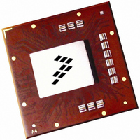
MPC8560CPX667JC Freescale Semiconductor, MPC8560CPX667JC Datasheet - Page 60

MPC8560CPX667JC
Manufacturer Part Number
MPC8560CPX667JC
Description
IC MPU PWRQUICC III 783-FCPBGA
Manufacturer
Freescale Semiconductor
Series
PowerQUICC IIIr
Specifications of MPC8560CPX667JC
Processor Type
MPC85xx PowerQUICC III 32-Bit
Speed
667MHz
Voltage
1.2V
Mounting Type
Surface Mount
Package / Case
783-FCPBGA
Core Size
32 Bit
Program Memory Size
64KB
Cpu Speed
667MHz
Embedded Interface Type
I2C, MII, SPI, TDM, UTOPIA
Digital Ic Case Style
BGA
No. Of Pins
783
Rohs Compliant
No
Family Name
MPC85XX
Device Core
PowerQUICC III
Device Core Size
32b
Frequency (max)
667MHz
Instruction Set Architecture
RISC
Supply Voltage 1 (typ)
1.2V
Operating Supply Voltage (max)
1.26V
Operating Supply Voltage (min)
1.14V
Operating Temp Range
-40C to 105C
Operating Temperature Classification
Industrial
Mounting
Surface Mount
Pin Count
783
Package Type
FCBGA
For Use With
MPC8560ADS-BGA - BOARD APPLICATION DEV 8560
Lead Free Status / RoHS Status
Contains lead / RoHS non-compliant
Features
-
Lead Free Status / Rohs Status
Not Compliant
Available stocks
Company
Part Number
Manufacturer
Quantity
Price
Company:
Part Number:
MPC8560CPX667JC
Manufacturer:
Freescale Semiconductor
Quantity:
10 000
RapidIO
Figure 41
13.2 RapidIO AC Electrical Specifications
This section contains the AC electrical specifications for a RapidIO 8/16 LP-LVDS device. The interface
defined is a parallel differential low-power high-speed signal interface. Note that the source of the transmit
clock on the RapidIO interface is
default setting makes the core complex bus (CCB) clock the source of the transmit clock. See Chapter 4
of the Reference Manual for more details on reset configuration settings.
13.3 RapidIO Concepts and Definitions
This section specifies signals using differential voltages.
figure shows waveforms for either a transmitter output (TD and TD) or a receiver input (RD and RD). Each
signal swings between A volts and B volts where A > B. Using these waveforms, the definitions are as
follows:
60
•
•
•
•
The transmitter output and receiver input signals TD, TD, RD, and RD each have a peak-to-peak
swing of A-B volts.
The differential output signal of the transmitter, V
The differential input signal of the receiver, V
The differential output signal of the transmitter or input signal of the receiver, ranges from
A – B volts to – (A – B) volts.
shows the DC driver signal levels.
–V + ΔV
–V – ΔV
Note: V
V
OD
OD
OD
OA
–V
= V
V
refers to voltage at output A; V
OA
MPC8560 Integrated Processor Hardware Specifications, Rev. 4.2
– V
Differential Specifications
OB
V
V
OA
OB
dependent o
(b)
Figure 41. DC Driver Signal Levels
–247 mV
–454 mV
454 mV
247 mV
R
(no m)
100 Ω
n the settings of the LGPL[0:1] signals at reset. Note that the
TERM
(a)
OB
refers to voltage at output B.
V
V
OHD
OLD
ID
, is defined as V
Figure 42
V
V
V
OD
OSCM
OHCM
OLCM
, is defined as V
0
= (V
Common-Mode Specifications
shows how the signals are defined. The
V
OA
+ V
RD
V
OB
OD
)/2
– V
= V
TD
(c)
OA
RD
– V
– V
.
1.375 V
1.125 V
TD
Freescale Semiconductor
OB
.
ΔV
OS


