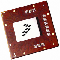
MPC8560CPX667JC Freescale Semiconductor, MPC8560CPX667JC Datasheet - Page 9

MPC8560CPX667JC
Manufacturer Part Number
MPC8560CPX667JC
Description
IC MPU PWRQUICC III 783-FCPBGA
Manufacturer
Freescale Semiconductor
Series
PowerQUICC IIIr
Specifications of MPC8560CPX667JC
Processor Type
MPC85xx PowerQUICC III 32-Bit
Speed
667MHz
Voltage
1.2V
Mounting Type
Surface Mount
Package / Case
783-FCPBGA
Core Size
32 Bit
Program Memory Size
64KB
Cpu Speed
667MHz
Embedded Interface Type
I2C, MII, SPI, TDM, UTOPIA
Digital Ic Case Style
BGA
No. Of Pins
783
Rohs Compliant
No
Family Name
MPC85XX
Device Core
PowerQUICC III
Device Core Size
32b
Frequency (max)
667MHz
Instruction Set Architecture
RISC
Supply Voltage 1 (typ)
1.2V
Operating Supply Voltage (max)
1.26V
Operating Supply Voltage (min)
1.14V
Operating Temp Range
-40C to 105C
Operating Temperature Classification
Industrial
Mounting
Surface Mount
Pin Count
783
Package Type
FCBGA
For Use With
MPC8560ADS-BGA - BOARD APPLICATION DEV 8560
Lead Free Status / RoHS Status
Contains lead / RoHS non-compliant
Features
-
Lead Free Status / Rohs Status
Not Compliant
Available stocks
Company
Part Number
Manufacturer
Quantity
Price
Company:
Part Number:
MPC8560CPX667JC
Manufacturer:
Freescale Semiconductor
Quantity:
10 000
2.1.2 Power Sequencing
The MPC8560 requires its power rails to be applied in a specific sequence in order to ensure proper device
operation. These requirements are as follows for power up:
Items on the same line have no ordering requirement with respect to one another. Items on separate lines
must be ordered sequentially such that voltage rails on a previous step must reach 90 percent of their value
before the voltage rails on the current step reach 10 percent of theirs.
Freescale Semiconductor
DDR DRAM I/O voltage
Three-speed Ethernet I/O voltage
CPM, PCI/PCI-X, local bus, RapidIO, 10/100 Ethernet,MII
management, DUART, system control and power management,
I
Input voltage
Storage temperature range
Notes:
1. Functional and tested operating conditions are given in
2. Caution: MV
3. Caution: OV
4. Caution: LV
5. (M,L,O)V
6. OV
2
C, and JTAG I/O voltage
functional operation at the maximums is not guaranteed. Stresses beyond those listed may affect device reliability or cause
permanent damage to the device.
power-on reset and power-down sequences.
power-on reset and power-down sequences.
power-on reset and power-down sequences.
shown in
1. V
2. GV
IN
on the PCI interface may overshoot/undershoot according to the PCI Electrical Specification for 3.3-V operation, as
DD
IN
Figure
DD
, AV
and MV
IN
IN
, LV
IN
must not exceed LV
must not exceed OV
must not exceed GV
DD
3.
DD
REF
, OV
Characteristic
may overshoot/undershoot to a voltage and for a maximum duration as shown in
MPC8560 Integrated Processor Hardware Specifications, Rev. 4.2
DD
DDR DRAM signals
DDR DRAM reference
Three-speed Ethernet signals
CPM, Local bus, RapidIO, 10/100
Ethernet, SYSCLK, system
control and power management,
I
PCI/PCI-X
Table 1. Absolute Maximum Ratings
2
C, and JTAG signals
(I/O supplies)
DD
DD
DD
by more than 0.3 V. This limit may be exceeded for a maximum of 20 ms during
by more than 0.3 V. This limit may be exceeded for a maximum of 20 ms during
by more than 0.3 V. This limit may be exceeded for a maximum of 20 ms during
Table
2. Absolute maximum ratings are stress ratings only, and
Symbol
MV
GV
OV
MV
LV
OV
OV
T
LV
STG
DD
REF
DD
DD
IN
IN
IN
IN
1
(continued)
–0.3 to (GV
–0.3 to (GV
–0.3 to (OV
–0.3 to (OV
–0.3 to (LV
–0.3 to 3.63
–0.3 to 3.63
–0.3 to 2.75
–0.3 to 3.63
Max Value
–55 to 150
DD
DD
DD
DD
DD
+ 0.3)
+ 0.3)
+ 0.3)
+ 0.3)
+ 0.3)
Electrical Characteristics
Unit
Figure
°C
V
V
V
V
V
V
V
V
2.
Notes
2, 5
2, 5
4, 5
—
—
—
3
5
6
9


