PRIXP425BB Intel, PRIXP425BB Datasheet - Page 4
PRIXP425BB
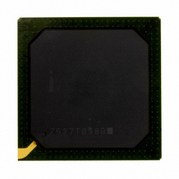
Manufacturer Part Number
PRIXP425BB
Description
IC NETWRK PROCESSR 266MHZ 492BGA
Manufacturer
Intel
Specifications of PRIXP425BB
Processor Type
Network
Features
XScale Core
Speed
266MHz
Voltage
1.3V
Mounting Type
Surface Mount
Package / Case
492-BGA
Lead Free Status / RoHS Status
Lead free / RoHS Compliant
Other names
869046


4.0
5.0
6.0
7.0
A
Intel
Hardware Design Guidelines
4
®
IXP42X Product Line of Network Processors and IXC1100 Control Plane Processor
3.12
3.13
PBGA Package..........................................................................................................55
4.1
4.2
General PCB Guide ...................................................................................................57
5.1
5.2
5.3
5.4
5.5
General Layout and Routing Guide ...........................................................................61
6.1
6.2
6.3
6.4
Critical Routing Topologies ......................................................................................73
7.1
7.2
A.1
A.2
A.3
A.4
A.5
A.6
A.7
A.8
Design Checklist......................................................................................................81
3.11.1 Interface Signals ....................................................................................48
3.11.2 Pull-Up/Down Resistors ...........................................................................48
Clock ...............................................................................................................48
3.12.1 Clock Signals .........................................................................................49
3.12.2 Using Oscillator ......................................................................................49
3.12.3 Design Notes..........................................................................................49
3.12.4 Block Diagram........................................................................................50
Power ..............................................................................................................50
3.13.1 Power Supply Requirements .....................................................................51
3.13.2 +3.3 V DC .............................................................................................51
3.13.3 +1.3 V DC .............................................................................................51
3.13.4 Power Up...............................................................................................51
PBGA Package Overview .....................................................................................55
Signal Grouping.................................................................................................55
PCB Overview ...................................................................................................57
General Recommendations..................................................................................57
Component Selection .........................................................................................57
Component Placement........................................................................................57
Stack Up Selection .............................................................................................58
Overview ..........................................................................................................61
General Layout Guidelines...................................................................................61
6.2.1
General Routing Guides ......................................................................................63
6.3.1
6.3.2
6.3.3
6.3.4
6.3.5
6.3.6
6.3.7
Devices’ Decoupling ...........................................................................................70
6.4.1
PC133 SDRAM Topologies ...................................................................................73
7.1.1
PCI Topologies ..................................................................................................75
7.2.1
7.2.2
7.2.3
Checklist ..........................................................................................................81
SDRAM Interface ...............................................................................................81
PCI Interface.....................................................................................................82
High-Speed Serial Interface ................................................................................83
MII Interface.....................................................................................................84
UTOPIA-2 Interface............................................................................................85
Expansion Bus Interface .....................................................................................86
A.7.1
UART Interface ..................................................................................................88
General Component Spacing ....................................................................62
Clock Signal Considerations......................................................................65
LAN Signal Considerations........................................................................66
USB Considerations.................................................................................67
Crosstalk ...............................................................................................67
EMI Design Considerations .......................................................................68
Trace Impedance ....................................................................................69
Power and Decoupling .............................................................................69
General Decoupling/Bypass Guidelines.......................................................70
PC 133 SDRAM Clock...............................................................................74
Trace Length Limits.................................................................................78
Routing Guidelines ..................................................................................78
Signal Loading........................................................................................79
Expansion Bus Configuration Strappings ....................................................87
Intel
®
IXP42X product line and IXC1100 control plane processors—Contents
Document Number: 252817-008US
December 2007
Related parts for PRIXP425BB
Image
Part Number
Description
Manufacturer
Datasheet
Request
R

Part Number:
Description:
Microprocessor: Intel Celeron M Processor 320 and Ultra Low Voltage Intel Celeron M Processor at 600MHz
Manufacturer:
Intel Corporation
Part Number:
Description:
Intel 82550 Fast Ethernet Multifunction PCI/CardBus Controller
Manufacturer:
Intel Corporation
Datasheet:
Part Number:
Description:
Intel StrataFlash memory 32 Mbit. Access speed 120 ns
Manufacturer:
Intel Corporation
Datasheet:
Part Number:
Description:
Intel StrataFlash memory 32 Mbit. Access speed 120 ns
Manufacturer:
Intel Corporation
Datasheet:
Part Number:
Description:
Intel StrataFlash memory 64 Mbit. Access speed 150 ns
Manufacturer:
Intel Corporation
Datasheet:
Part Number:
Description:
Intel StrataFlash memory 32 Mbit. Access speed 100 ns
Manufacturer:
Intel Corporation
Datasheet:
Part Number:
Description:
DA28F640J5A-1505 Volt Intel StrataFlash Memory
Manufacturer:
Intel Corporation
Datasheet:
Part Number:
Description:
5 Volt Intel StrataFlash?? Memory
Manufacturer:
Intel Corporation
Datasheet:
Part Number:
Description:
5 Volt Intel StrataFlash?? Memory
Manufacturer:
Intel Corporation
Part Number:
Description:
Intel 6300ESB I/O Controller Hub
Manufacturer:
Intel Corporation
Datasheet:
Part Number:
Description:
Intel 82801DB I/O Controller Hub (ICH4), Pb-Free SLI
Manufacturer:
Intel Corporation
Datasheet:
Part Number:
Description:
Intel 82801FB I/O Controller Hub (ICH6)
Manufacturer:
Intel Corporation
Datasheet:
Part Number:
Description:
Intel Strataflash Memory28F128J3 28F640J3 28F320J3
Manufacturer:
Intel Corporation
Datasheet:
Part Number:
Description:
Controllers, Intel 430TX PCIset: 82439TX System Controller (MTXC)
Manufacturer:
Intel Corporation