USBN9603SLBX National Semiconductor, USBN9603SLBX Datasheet - Page 30
USBN9603SLBX
Manufacturer Part Number
USBN9603SLBX
Description
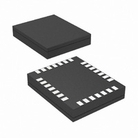
IC CTRLR FULL SPEED 28-LAMCSP
Manufacturer
National Semiconductor
Datasheet
1.USBN9604-28MNOPB.pdf
(60 pages)
Specifications of USBN9603SLBX
Controller Type
USB 2.0 Controller
Interface
Parallel/Serial
Voltage - Supply
3 V ~ 5.5 V
Current - Supply
30mA
Operating Temperature
0°C ~ 70°C
Mounting Type
Surface Mount
Package / Case
28-Laminate CSP
For Use With
USBN9604-HS-EB - KIT NODE CONTROLLER SAMPLE
Lead Free Status / RoHS Status
Lead free / RoHS Compliant
Other names
USBN9603SLBX
USBN9603SLBX/NOPB
USBN9603SLBXTR
USBN9603SLBX/NOPB
USBN9603SLBXTR
Available stocks
Company
Part Number
Manufacturer
Quantity
Price


www.national.com
7.0 Register Set
The device has a set of memory-mapped registers that can be read from/written to control the USB interface. Some register
bits are reserved; reading from these bits returns undefined data. Reserved register bits should always be written with 0.
The following conventions are used to describe the register format:
7.1 CONTROL REGISTERS
7.1.1
SRST
Software Reset. Setting this bit causes a software reset of the device. This reset is equivalent to a hardware reset except
that the Clock Configuration (CCONF) register is unaffected. All registers revert to their default values. This bit is cleared
automatically upon completion of the initiated reset.
VGE
Voltage Regulator Enable. Setting this bit enables the internal 3.3V voltage regulator. This bit is hardware reset only to a 0,
disabling the internal 3.3V regulator by default. When the internal 3.3V regulator is disabled, the device is effectively discon-
nected from USB. Upon power-up, the firmware may perform any needed initialization (such as power-on self test) and then
set the VGE bit. Until the VGE bit is set, the upstream hub port does not detect the device presence.
If the VGE bit is reset an external 3.3V power supply may be used on the V3.3 pin.
NAT
Node Attached. This bit indicates that this node is ready to be detected as attached to USB. When reset the transceiver
forces SE0 on the USB port to prevent the hub (to which this node is connected to) from detecting an attach event. After
reset, this bit is left cleared to give the device time before it must respond to commands. After this bit is set, the device no
longer drives the USB and should be ready to receive Reset signaling from the hub.
The NAT bit should be set by the firmware if an external 3.3V supply has been provided to the V3.3 pin, or at least 1 mS
after the VGE bit is set (in the latter case, the delay allows the internal regulator sufficient time to stabilize).
INTOC
Interrupt Output Control. These bits control interrupt ouput according to the following table.
Corresponding FIFO
Main Control Register (MCNTRL)
Bit Mnemonic
Register Type
Reset Value
Bit Number
bit 7
0
INTOC1-0
r/w
bit 7
bit 6
0
r
w
r/w
CoR = Cleared on read
CoW = Cleared on write if written with 0; writing a 1 has no effect
HW
bit 6
bit 5
= Read only
= Write only
= Read and write by firmware
= Modified by the device and by firmware
Corresponding FIFO types and numbers, where relevant
Reserved
-
-
bit 5
bit 4
30
reset values, where relevant
Abbreviated bit/field names
bit 3
NAT
bit 4
r/w
0
bit 2
VGE
bit 3
r/w
0
Reserved
bit 1
bit 2
SRST
bit 0
r/w
bit 1
0
bit 0
Related parts for USBN9603SLBX
Image
Part Number
Description
Manufacturer
Datasheet
Request
R

Part Number:
Description:
IC CONTROLLER USB 28-SOIC
Manufacturer:
National Semiconductor
Datasheet:

Part Number:
Description:
USB Controller IC
Manufacturer:
National Semiconductor
Datasheet:
Part Number:
Description:
IC CTRLR FULL SPD FUNC 28-SOIC
Manufacturer:
National Semiconductor
Datasheet:

Part Number:
Description:
USBN9603 Universal Serial Bus Full Speed Function Controller with Enhanced DMA Support
Manufacturer:
National Semiconductor
Datasheet:
Part Number:
Description:
Universal Serial Bus Full Speed Node Controller with Enhanced DMA Support
Manufacturer:
National Semiconductor
Part Number:
Description:
USBN9603/USBN9604 Universal Serial Bus Full Speed Node Controller with Enhanced DMA Support
Manufacturer:
National Semiconductor
Datasheet:
Part Number:
Description:
National Semiconductor [8-Bit D/A Converter]
Manufacturer:
National Semiconductor
Datasheet:
Part Number:
Description:
National Semiconductor [Media Coprocessor]
Manufacturer:
National Semiconductor
Datasheet:
Part Number:
Description:
Digitally Controlled Tone and Volume Circuit with Stereo Audio Power Amplifier, Microphone Preamp Stage and National 3D Sound
Manufacturer:
National Semiconductor
Datasheet:
Part Number:
Description:
Digitally Controlled Tone and Volume Circuit with Stereo Audio Power Amplifier, Microphone Preamp Stage and National 3D Sound
Manufacturer:
National Semiconductor
Datasheet:
Part Number:
Description:
AC97 Rev 2 Codec with Sample Rate Conversion and National 3D Sound
Manufacturer:
National Semiconductor
Part Number:
Description:
Manufacturer:
National Semiconductor
Datasheet:
Part Number:
Description:
Manufacturer:
National Semiconductor
Datasheet: