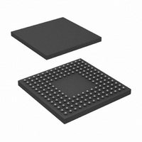
DP83815DUJB/NOPB National Semiconductor, DP83815DUJB/NOPB Datasheet - Page 16

DP83815DUJB/NOPB
Manufacturer Part Number
DP83815DUJB/NOPB
Description
IC MEDIA ACCESS CONTROL 160-LBGA
Manufacturer
National Semiconductor
Datasheet
1.DP83815DVNGNOPB.pdf
(108 pages)
Specifications of DP83815DUJB/NOPB
Controller Type
Ethernet Controller, MAC/BIU
Interface
PCI
Voltage - Supply
3.3V
Current - Supply
170mA
Operating Temperature
0°C ~ 70°C
Mounting Type
Surface Mount
Package / Case
160-LBGA
Lead Free Status / RoHS Status
Lead free / RoHS Compliant
Other names
*DP83815DUJB
*DP83815DUJB/NOPB
DP83815DUJB
*DP83815DUJB/NOPB
DP83815DUJB
Available stocks
Company
Part Number
Manufacturer
Quantity
Price
Company:
Part Number:
DP83815DUJB/NOPB
Manufacturer:
Texas Instruments
Quantity:
10 000
Subject to change without notice.
3.0 Functional Description
The standard 802.3 Ethernet packet consists of the
following fields: Preamble (PA), Start of Frame Delimiter
(SFD), Destination Address (DA), Source Address (SA),
Length (LEN), Data and Frame Check Sequence (FCS). All
fields are fixed length except for the data field. During
reception, the PA, SFD and FCS are stripped. During
transmission, the DP83815 generates and appends the
PA, SFD and FCS.
3.2.4 MIB
The MIB block contains counters to track certain media
events required by the management specifications RFC
1213 (MIB II), RFC 1398 (Ether-like MIB), and IEEE 802.3
LME. The counters provided are for events which are either
difficult or impossible to be intercepted directly by software.
Not all counters are implemented, however required
counters can be calculated from the counters provided.
3.3 Interface Definitions
3.3.1 PCI System Bus
This interface allows direct connection of the DP83815 to a
33 MHz PCI system bus. The DP83815 supports zero wait
state data transfers with burst sizes up to 128 dwords. The
DP83815 conforms to 3.3V AC/DC specifications, but has
5V tolerant inputs.
Note: B = Bytes
60b
PA
b = bits
Figure 3-3 Ethernet Packet Format
SFD
4b
DA
6B
SA
6B
LEN
2B
46B-1500B
(Continued)
Data
FCS
4B
16
3.3.2 Boot PROM
The BIOS ROM interface allows the DP83815 to read from
and write data to an external ROM/Flash device.
3.3.3 EEPROM
The DP83815 supports the attachment of an external
EEPROM. The EEPROM interface provides the ability for
the DP83815 to read from and write data to an external
serial EEPROM device. The DP83815 will auto-load values
from the EEPROM to certain fields in PCI configuration
space and operational space and perform a checksum to
verify that the data is valid. Values in the external EEPROM
allow default fields in PCI configuration space and I/O
space to be overridden following a hardware reset. If the
EEPROM is not present, the DP83815 initialization uses
default values for the appropriate Configuration and
Operational Registers. Software can read and write to the
EEPROM using “bit-bang” accesses via the EEPROM
Access Register (MEAR).
3.3.4 Clock
The clock interface provides the 25 MHz clock reference
input for the DP83815 IC. The X1 and X2 pin capacitances
are 4.5 + 1.0pF. The X1 input signal amplitude should be
approximately 1V. This interface supports operation from a
25 MHz, 50 ppm CMOS oscillator, or a 25 MHz, 50 ppm,
parallel, 20 pF load, < 40 Ω ESR crystal resonator. A 20pF
crystal resonator would require C1 and C2 load capacitors
of 27-33pF each.
Rev O
www.national.com


