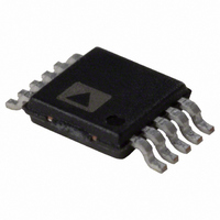
AD9833BRMZ Analog Devices Inc, AD9833BRMZ Datasheet - Page 17

AD9833BRMZ
Manufacturer Part Number
AD9833BRMZ
Description
IC WAVEFORM GENERTR PROG 10-MSOP
Manufacturer
Analog Devices Inc
Specifications of AD9833BRMZ
Resolution (bits)
10 b
Master Fclk
25MHz
Tuning Word Width (bits)
28 b
Voltage - Supply
2.3 V ~ 5.5 V
Operating Temperature
-40°C ~ 105°C
Mounting Type
Surface Mount
Package / Case
10-MSOP, Micro10™, 10-uMAX, 10-uSOP
Ic Function
Direct Digital Synthesizer
Supply Voltage Range
2.3V To 5.5V
Operating Temperature Range
-40°C To +105°C
Digital Ic Case Style
MSOP
No. Of Pins
10
Msl
MSL 3 - 168 Hours
Supplier Package
MSOP
Resolution
10 Bit
Maximum Input Frequency
25 MHz
Tuning Word Width
28 Bit
Minimum Operating Supply Voltage
2.3 V
Typical Operating Supply Voltage
2.5|3.3|5 V
Maximum Operating Supply Voltage
5.5 V
Minimum Operating Temperature
-40 °C
Maximum Operating Temperature
105 °C
Lead Free Status / RoHS Status
Lead free / RoHS Compliant
For Use With
EVAL-AD9833EBZ - BOARD EVAL FOR AD9833
Lead Free Status / Rohs Status
RoHS Compliant part
Electrostatic Device
Available stocks
Company
Part Number
Manufacturer
Quantity
Price
Company:
Part Number:
AD9833BRMZ
Manufacturer:
MICRON
Quantity:
2 154
Company:
Part Number:
AD9833BRMZ
Manufacturer:
ADI
Quantity:
5 000
Part Number:
AD9833BRMZ
Manufacturer:
ADI/亚德诺
Quantity:
20 000
Part Number:
AD9833BRMZ-REEL
Manufacturer:
ADI/亚德诺
Quantity:
20 000
Company:
Part Number:
AD9833BRMZ-REEL7
Manufacturer:
AD
Quantity:
14 592
Part Number:
AD9833BRMZ-REEL7
Manufacturer:
ADI/亚德诺
Quantity:
20 000
APPLICATIONS INFORMATION
Because of the various output options available from the part,
the AD9833 can be configured to suit a wide variety of applications.
One of the areas where the AD9833 is suitable is in modulation
applications. The part can be used to perform simple modulation,
such as FSK. More complex modulation schemes, such as
GMSK and QPSK, can also be implemented using the AD9833.
In an FSK application, the two frequency registers of the AD9833
are loaded with different values. One frequency represents the
space frequency, while the other represents the mark frequency.
Using the FSELECT bit in the control register of the AD9833, the
user can modulate the carrier frequency between the two values.
The AD9833 has two phase registers, which enables the part to
perform PSK. With phase-shift keying, the carrier frequency is
phase shifted, the phase being altered by an amount that is
related to the bit stream being input to the modulator.
The AD9833 is also suitable for signal generator applications.
Because the MSB of the DAC data is available at the VOUT pin,
the device can be used to generate a square wave.
With its low current consumption, the part is suitable for
applications in which it can be used as a local oscillator.
Rev. C | Page 17 of 24
GROUNDING AND LAYOUT
The printed circuit board (PCB) that houses the AD9833 should be
designed so that the analog and digital sections are separated
and confined to certain areas of the board. This facilitates the
use of ground planes that can be separated easily. A minimum
etch technique is generally best for ground planes because it gives
the best shielding. Digital and analog ground planes should be
joined in one place only. If the AD9833 is the only device requiring
an AGND-to-DGND connection, then the ground planes should
be connected at the AGND and DGND pins of the AD9833. If
the AD9833 is in a system where multiple devices require AGND-
to-DGND connections, the connection should be made at one
point only, a star ground point that should be established as
close as possible to the AD9833.
Avoid running digital lines under the device as these couple noise
onto the die. The analog ground plane should be allowed to run
under the AD9833 to avoid noise coupling. The power supply
lines to the AD9833 should use as large a track as possible to
provide low impedance paths and reduce the effects of glitches
on the power supply line. Fast switching signals, such as clocks,
should be shielded with digital ground to avoid radiating noise
to other sections of the board. Avoid crossover of digital and
analog signals. Traces on opposite sides of the board should run at
right angles to each other. This reduces the effects of feedthrough
through the board. A microstrip technique is by far the best, but it
is not always possible with a double-sided board. In this technique,
the component side of the board is dedicated to ground planes,
and signals are placed on the other side.
Good decoupling is important. The AD9833 should have supply
bypassing of 0.1 μF ceramic capacitors in parallel with 10 μF
tantalum capacitors. To achieve the best from the decoupling
capacitors, they should be placed as close as possible to the
device, ideally right up against the device.
AD9833


