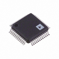
AD9830ASTZ Analog Devices Inc, AD9830ASTZ Datasheet - Page 12

AD9830ASTZ
Manufacturer Part Number
AD9830ASTZ
Description
IC DDS 10BIT 50MHZ CMOS 48-TQFP
Manufacturer
Analog Devices Inc
Datasheet
1.AD9830ASTZ.pdf
(16 pages)
Specifications of AD9830ASTZ
Resolution (bits)
10 b
Master Fclk
50MHz
Tuning Word Width (bits)
32 b
Voltage - Supply
4.75 V ~ 5.25 V
Operating Temperature
-40°C ~ 85°C
Mounting Type
Surface Mount
Package / Case
48-TQFP, 48-VQFP
Pll Type
Direct Digital Synthesis
Frequency
50MHz
Supply Current
60mA
Supply Voltage Range
4.75V To 5.25V
Digital Ic Case Style
TQFP
No. Of Pins
48
Operating Temperature Range
-40°C To +85°C
Ic Function
Direct Digital Synthesizer
Svhc
No SVHC (15-Dec-2010)
Rohs Compliant
Yes
Bandwidth
50MHz
Lead Free Status / RoHS Status
Lead free / RoHS Compliant
For Use With
EVAL-AD9830EBZ - BOARD EVALUATION AD9830
Lead Free Status / RoHS Status
Lead free / RoHS Compliant, Lead free / RoHS Compliant
Available stocks
Company
Part Number
Manufacturer
Quantity
Price
Company:
Part Number:
AD9830ASTZ
Manufacturer:
Analog Devices Inc
Quantity:
10 000
Company:
Part Number:
AD9830ASTZ-REEL
Manufacturer:
Analog Devices Inc
Quantity:
10 000
AD9830
APPLICATIONS
The AD9830 contains functions which make it suitable for
modulation applications. The part can be used to perform
simple modulation such as FSK. More complex modulation
schemes such as GMSK and QPSK can also be implemented
using the AD9830. In a FSK application, the two frequency reg-
isters of the AD9830 are loaded with different values, one fre-
quency will represent the space frequency while the other will
represent the mark frequency. The digital data stream is fed to
the FSELECT pin which will cause the AD9830 to modulate
the carrier frequency between the two values.
The AD9830 has four phase registers which enable the part to
perform PSK. With phase shift keying, the carrier frequency is
phase shifted, the phase being altered by an amount which is
ANTENNA
RFLO
PRUP
VPS2
VPS1
RFHI
AD9830
10 BITS
51
51
LOIP
R
1k
FILTER
SET
0.1µF
GENERATOR
MIDPOINT
Figure 24. AD9830 and AD6459 Receiver Circuit
CIRCUIT
BIAS
BIAS
MXOM
MXOP
COM1
BANDPASS
FILTER
COM2
–12–
related to the bit stream being input to the modulator. The
presence of four shift registers eases the interaction needed
between the DSP and the AD9830.
The frequency and phase registers can be written to continuously,
if required. The maximum update rate equals the frequency of
the MCLK. However, if a selected register is loaded with a new
word, there will be a delay of 6 MCLK cycles before the analog
output will change accordingly.
The AD9830 is also suitable for signal generator applications.
With its low current consumption, the part is suitable for
mobile applications in which it can be used as a local oscillator.
Figure 24 shows the interface between the AD9830 and AD6459
which is a down converter used on the receive side of mobile
phones or basestations.
IFIM
IFIP
AD6459
COMPENSATION
GAIN TC
PLL
0
90
IRxP
IRxN
FREF
FLTR
QRxP
QRxN
GAIN
GREF
REV. A


