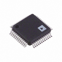
AD9830ASTZ Analog Devices Inc, AD9830ASTZ Datasheet - Page 13

AD9830ASTZ
Manufacturer Part Number
AD9830ASTZ
Description
IC DDS 10BIT 50MHZ CMOS 48-TQFP
Manufacturer
Analog Devices Inc
Datasheet
1.AD9830ASTZ.pdf
(16 pages)
Specifications of AD9830ASTZ
Resolution (bits)
10 b
Master Fclk
50MHz
Tuning Word Width (bits)
32 b
Voltage - Supply
4.75 V ~ 5.25 V
Operating Temperature
-40°C ~ 85°C
Mounting Type
Surface Mount
Package / Case
48-TQFP, 48-VQFP
Pll Type
Direct Digital Synthesis
Frequency
50MHz
Supply Current
60mA
Supply Voltage Range
4.75V To 5.25V
Digital Ic Case Style
TQFP
No. Of Pins
48
Operating Temperature Range
-40°C To +85°C
Ic Function
Direct Digital Synthesizer
Svhc
No SVHC (15-Dec-2010)
Rohs Compliant
Yes
Bandwidth
50MHz
Lead Free Status / RoHS Status
Lead free / RoHS Compliant
For Use With
EVAL-AD9830EBZ - BOARD EVALUATION AD9830
Lead Free Status / RoHS Status
Lead free / RoHS Compliant, Lead free / RoHS Compliant
Available stocks
Company
Part Number
Manufacturer
Quantity
Price
Company:
Part Number:
AD9830ASTZ
Manufacturer:
Analog Devices Inc
Quantity:
10 000
Company:
Part Number:
AD9830ASTZ-REEL
Manufacturer:
Analog Devices Inc
Quantity:
10 000
REV. A
Grounding and Layout
The printed circuit board that houses the AD9830 should be
designed so that the analog and digital sections are separated
and confined to certain areas of the board. This facilitates the
use of ground planes which can be separated easily. A mini-
mum etch technique is generally best for ground planes as it
gives the best shielding. Digital and analog ground planes
should only be joined in one place. If the AD9830 is the only
device requiring an AGND to DGND connection, then the
ground planes should be connected at the AGND and DGND
pins of the AD9830. If the AD9830 is in a system where mul-
tiple devices require AGND to DGND connections, the con-
nection should be made at one point only, a star ground point
that should be established as close as possible to the AD9830.
Avoid running digital lines under the device as these will couple
noise onto the die. The analog ground plane should be allowed
to run under the AD9830 to avoid noise coupling. The power
supply lines to the AD9830 should use as large a track as is pos-
sible to provide low impedance paths and reduce the effects of
glitches on the power supply line. Fast switching signals like
clocks should be shielded with digital ground to avoid radiating
noise to other sections of the board. Avoid crossover of digital
and analog signals. Traces on opposite sides of the board
should run at right angles to each other. This will reduce the ef-
fects of feedthrough through the board. A microstrip technique
is by far the best but is not always possible with a double-sided
board. In this technique, the component side of the board is
dedicated to ground planes while signals are placed on the other
side.
Good decoupling is important. The analog and digital supplies
to the AD9830 are independent and separately pinned out to
minimize coupling between analog and digital sections of the
device. All analog and digital supplies should be decoupled to
AGND and DGND respectively with 0.1 F ceramic capacitors
in parallel with 10 F tantalum capacitors. To achieve the best
from the decoupling capacitors, they should be placed as close
as possible to the device, ideally right up against the device. In
systems where a common supply is used to drive both the AVDD
and DVDD of the AD9830, it is recommended that the system’s
AVDD supply be used. This supply should have the recom-
mended analog supply decoupling between the AVDD pins of
the AD9830 and AGND and the recommended digital supply
decoupling capacitors between the DVDD pins and DGND.
–13–
AD9830 Evaluation Board
The AD9830 Evaluation Board allows designers to evaluate the
high performance AD9830 DDS Modulator with a minimum of
effort.
To prove that this device will meet the user’s waveform synthesis
requirements, the user only requires a +5 V power supply, an
IBM-compatible PC and a spectrum analyzer along with the
evaluation board. The evaluation setup is shown below.
The DDS Evaluation kit includes a populated, tested AD9830
printed circuit board along with software which controls the
AD9830 in a Windows environment.
Using the AD9830 Evaluation Board
The AD9830 Evaluation kit is a test system designed to simplify
the evaluation of the AD9830. Provisions to control the AD9830
from the printer port of an IBM-compatible PC are included
along with the necessary software. An application note is also
available with the evaluation board which gives information on
operating the evaluation board.
Prototyping Area
An area is available on the evaluation board where the user can
add additional circuits to the evaluation test set. Users may
want to build custom analog filters for the outputs or add buf-
fers and operational amplifiers which are to be used in the final
application.
XO vs. External Clock
The AD9830 can operate with master clocks up to 50 MHz. A
50 MHz oscillator is included on the evaluation board. How-
ever, this oscillator can be removed and an external CMOS
clock connected to the part, if required.
Power Supply
Power to the AD9830 evaluation board must be provided exter-
nally through the pin connections. The power leads should be
twisted to reduce ground loops.
AD9830.EXE
Figure 25. AD9830 Evaluation Board Setup
IBM COMPATIBLE PC
PARALLEL PORT
PRINTER CABLE
CENTRONICS
AD9830
AD9830 EVALUATION
BOARD


