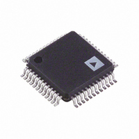
AD9831ASTZ Analog Devices Inc, AD9831ASTZ Datasheet - Page 2

AD9831ASTZ
Manufacturer Part Number
AD9831ASTZ
Description
IC DDS 10BIT 25MHZ CMOS 48-LQFP
Manufacturer
Analog Devices Inc
Datasheet
1.AD9831ASTZ-REEL.pdf
(7 pages)
Specifications of AD9831ASTZ
Resolution (bits)
10 b
Master Fclk
25MHz
Tuning Word Width (bits)
32 b
Voltage - Supply
2.97 V ~ 5.5 V
Operating Temperature
-40°C ~ 85°C
Mounting Type
Surface Mount
Package / Case
48-TQFP, 48-VQFP
Pll Type
Direct Digital Synthesis
Frequency
25MHz
Supply Current
15mA
Supply Voltage Range
2.97V To 5.5V
Digital Ic Case Style
TQFP
No. Of Pins
48
Operating Temperature Range
-40°C To +85°C
Lead Free Status / RoHS Status
Lead free / RoHS Compliant
For Use With
EVAL-AD9831EBZ - BOARD EVALUATION AD9831
Lead Free Status / RoHS Status
Lead free / RoHS Compliant, Lead free / RoHS Compliant
Available stocks
Company
Part Number
Manufacturer
Quantity
Price
Company:
Part Number:
AD9831ASTZ
Manufacturer:
ADI
Quantity:
217
Company:
Part Number:
AD9831ASTZ
Manufacturer:
Analog Devices Inc
Quantity:
10 000
Part Number:
AD9831ASTZ
Manufacturer:
ADI/亚德诺
Quantity:
20 000
Company:
Part Number:
AD9831ASTZ-REEL
Manufacturer:
Analog Devices Inc
Quantity:
10 000
EVAL-AD9831EB
Link and Switch Options
There are five link options which must be set for the required operating setup before using the evaluation board. The functions
of these options are outlined below.
Link No.
LK1
LK2
LK3
LK4
LK5
Function
The PSEL1 input can be controlled by the user via a BNC connector or, alternatively, by switch SW.
When LK1 is arranged so that PSEL1 is connected to SW, the user can control the PSEL1 signal using the
double throw switch.
Alternatively, PSEL1 can be tied to a BNC connector by altering LK1 so that the user can provide the PSEL1
control from a logic source.
The PSEL0 input can be controlled by the user via a BNC connector or, alternatively, by switch SW.
When LK2 is arranged so that PSEL0 is connected to SW, the user can control the PSEL0 signal using the
double throw switch.
Alternatively, PSEL0 can be tied to a BNC connector by altering LK2 so that the user can provide the PSEL0
control from a logic source.
The FSELECT input can be controlled by the user via a BNC connector or, alternatively, by switch SW.
When LK3 is arranged so that FSELECT is connected to SW, the user can control the FSELECT signal using
the double throw switch.
Alternatively, FSELECT can be tied to a BNC connector by altering LK3 so that the user can provide the
FSELECT control from a logic source.
LK4 is used to place the AD9831 in sleep mode.
When LK4 is connected so that
AD9831's internal clocks, REFOUT and the DAC are disabled.
When LK4 is connected so that
The reference to the AD9831 can be provided by the on-board reference, which is available at REFOUT, or an
external reference of nominal value 1.21 V can be used. When LK5 is closed, the on-board reference is used.
When this link is opened, REFIN is disconnected from REFOUT and the reference can be provided by the
user via a BNC connector.
SLEEP
SLEEP
is tied to DGND, the AD9831 is placed in sleep mode whereby the
is tied to DVDD, the AD9831 is powered up.
- 2 -
REV O


