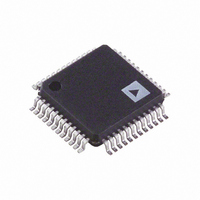
AD9831ASTZ Analog Devices Inc, AD9831ASTZ Datasheet - Page 5

AD9831ASTZ
Manufacturer Part Number
AD9831ASTZ
Description
IC DDS 10BIT 25MHZ CMOS 48-LQFP
Manufacturer
Analog Devices Inc
Datasheet
1.AD9831ASTZ-REEL.pdf
(7 pages)
Specifications of AD9831ASTZ
Resolution (bits)
10 b
Master Fclk
25MHz
Tuning Word Width (bits)
32 b
Voltage - Supply
2.97 V ~ 5.5 V
Operating Temperature
-40°C ~ 85°C
Mounting Type
Surface Mount
Package / Case
48-TQFP, 48-VQFP
Pll Type
Direct Digital Synthesis
Frequency
25MHz
Supply Current
15mA
Supply Voltage Range
2.97V To 5.5V
Digital Ic Case Style
TQFP
No. Of Pins
48
Operating Temperature Range
-40°C To +85°C
Lead Free Status / RoHS Status
Lead free / RoHS Compliant
For Use With
EVAL-AD9831EBZ - BOARD EVALUATION AD9831
Lead Free Status / RoHS Status
Lead free / RoHS Compliant, Lead free / RoHS Compliant
Available stocks
Company
Part Number
Manufacturer
Quantity
Price
Company:
Part Number:
AD9831ASTZ
Manufacturer:
ADI
Quantity:
217
Company:
Part Number:
AD9831ASTZ
Manufacturer:
Analog Devices Inc
Quantity:
10 000
Part Number:
AD9831ASTZ
Manufacturer:
ADI/亚德诺
Quantity:
20 000
Company:
Part Number:
AD9831ASTZ-REEL
Manufacturer:
Analog Devices Inc
Quantity:
10 000
Preliminary Technical Data
AD7002
EVAL-AD9831EB
SOFTWARE DESCRIPTION
Included in the EVAL-AD9831EB evaluation board package is a PC-compatible disk which contains software for controlling the
AD9831 using the printer port of a PC. The disk contains the executable program which runs under Windows and it is advised
that the user copy this file to the system hard disk to obtain optimum performance from the software.
PC Configuration
The executable program contains two menus. The first menu gives options on the type of PC being used. The printer port
needs to be configured correctly for one of the three different PC-types for interfacing to the AD9831. Choose the required
printer type from the menu. The PC printer port is now configured for operation with the AD9831 evaluation board.
Figure 2. Parallel Port Selection
Running the AD9831 Software
The second menu gives options for running the AD9831. All registers of the AD9831 can be written to using this software.
The MCLK frequency is set to 25 MHz by default in the program. However, the user has the capability of changing the MCLK
frequency. When the master clock has a frequency other than 25 MHz, the user can change the value of the MCLK frequency
in the program so that the software can correctly calculate the digital words corresponding to the different output frequencies.
The Frequency Registers are written to by writing in the required frequency in MHz to the PC. The AD9831 software will
calculate the corresponding word which will be written to the AD9831 and display the word in hex on the screen. The Phase
Registers are written to by writing in the required value in decimal to the PC. The software will then control the loading of this
information into the AD9831.
To write to a Phase Register, three transfers of data from the PC are needed since the PC uses 8-bit transfers. The 16 bit word
along with the address of the destination register is transferred from the PC to the AD9831. The sixteen bit word is split into
two 8-bit words (the 8 MSBs and the 8 LSBs). The first transfer of data involves transferring the 8 MSBs of the 16-bit word.
When these 8 bits are being transferred, a pulse is also generated on the LOAD pin so that the 8 bits of data are latched into U2
on the rising edge of LOAD.
During the second transfer, the 8 LSBs are transferred to U3, a pulse being generated on the LATCH pin so that these 8 bits are
latched into U3.
The third transfer involves transferring the address of the destination register (A0, A1 and A2). When the PC outputs the
address information (which is available on D0, D1 and D2 respectively), the PC also generates the
WR
pulse. On the rising
edge of
WR
, the 16 bits of data are read from the 74HC574 latches and the address of the destination register is read from the
data bus.
Because the Frequency Registers are 32 bits wide, there will be six transfers from the PC when these registers are being written
to. Writing the 16 LSBs to the Frequency Register involves transferring the destination register address (000 or 010) and the 16
bits of data. Similarly, the destination address for the 16 MSBs (001 or 011) and 16 bits of data need to be transferred when
writing to the 16 MSBs of the Frequency Register.
The logic inputs FSELECT, PSEL0 and PSEL1 are not controlled by the PC. These inputs can be controlled using the switch
SW or, alternatively, these inputs can be controlled using an external source via the BNC connectors.
- 5 -
REV O


