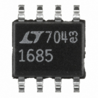
LTC1685CS8#PBF Linear Technology, LTC1685CS8#PBF Datasheet - Page 2

LTC1685CS8#PBF
Manufacturer Part Number
LTC1685CS8#PBF
Description
IC TXRX RS485 PREC DELAY 8-SOIC
Manufacturer
Linear Technology
Type
Transceiverr
Datasheet
1.LTC1685CS8PBF.pdf
(12 pages)
Specifications of LTC1685CS8#PBF
Number Of Drivers/receivers
1/1
Protocol
RS422, RS485
Voltage - Supply
4.75 V ~ 5.25 V
Mounting Type
Surface Mount
Package / Case
8-SOIC (3.9mm Width)
Lead Free Status / RoHS Status
Lead free / RoHS Compliant
Available stocks
Company
Part Number
Manufacturer
Quantity
Price
A
LTC1685
(Note 1)
Supply Voltage (V
Control Input Currents .................... – 100mA to 100mA
Control Input Voltages .................. – 0.5V to V
Driver Input Voltages .................... – 0.5V to V
Driver Output Voltages .................................. +12V/– 7V
Receiver Input Voltages ................................. +12V/– 7V
Receiver Output Voltages ............. – 0.5V to V
Receiver Input Differential ...................................... 10V
Short-Circuit Duration (Driver V
Receiver V
Operating Temperature Range
Storage Temperature Range ................ – 65 C to 150 C
Lead Temperature (Soldering, 10 sec)................. 300 C
DC ELECTRICAL CHARACTERISTICS
temperature range, otherwise specifications are at T
SYMBOL
V
V
V
V
V
I
I
V
V
V
I
I
I
2
IN1
IN2
OZR
DD
OSD1
OD1
OD2
OC
IH
IL
TH
OH
OL
V
V
BSOLUTE
OD
TH
V
LTC1685C ............................................... 0 C to 70 C
LTC1685I ............................................. –40 C to 85 C
OC
PARAMETER
Differential Driver Output (Unloaded)
Differential Driver Output (With Load)
Change in Magnitude of Driver Differential
Output Voltage for Complementary
Output States
Driver Common Mode Output Voltage
Change in Magnitude of Driver Common
Mode Output Voltage for Complementary
Output States
Input High Voltage
Input Low Voltage
Input Current
Input Current (A, B)
Differential Input Threshold Voltage
for Receiver
Receiver Input Hysteresis
Receiver Output High Voltage
Receiver Output Low Voltage
Three-State (High Impedance) Output
Current at Receiver
Supply Current
Driver Short-Circuit Current, V
OUT
: 0V to V
DD
W
) .............................................. 10V
A
DD
XI
) ............................... Indefinite
W
U
OUT
OUT
W
: – 7V to 10V,
= HIGH
R
A
TI
CONDITIONS
I
R = 50 (RS422)
R = 27 (RS485), Figure 1
R = 27 or 50 , Figure 1
R = 27 or 50 , V
R = 27 or 50 , Figure 1
DE, DI, RE
DE, DI, RE
DE, DI, RE
V
V
– 7V V
V
I
I
0.4V V
No Load, Pins 2, 3, 4 = 0V or V
V
OUT
OUT
OUT
U
A
A
CM
OUT
A
, V
, V
DD
DD
DD
= 25 C. V
G
= 0V
= 0
= – 4mA, V
= 4mA, V
B
B
= – 7V or 10V (Note 5)
= 12V, DE = 0, V
= – 7V, DE = 0, V
+ 0.5V
+ 0.5V
+ 0.5V
S
CM
OUT
12V
ID
DD
2.4V
ID
The
= – 300mV
= 5V 5%, unless otherwise noted. (Notes 2, 3)
= 300mV
DD
Consult factory for Military grade parts.
PACKAGE/ORDER I FOR ATIO
= 5V, Figure 1
denotes the specifications which apply over the full operating
DD
DD
= 0V or 5.25V
= 0V or 5.25V
RO
RE
DE
DI
DD
T
JMAX
1
2
3
4
8-LEAD PLASTIC SO
= 125 C,
S8 PACKAGE
TOP VIEW
D
R
JA
= 150 C/ W
8
7
6
5
V
B
A
GND
DD
– 500
– 0.3
MIN
1.5
3.5
– 1
– 1
2
2
2
U
TYP
S8 PART MARKING
4.8
25
7
ORDER PART
LTC1685CS8
LTC1685IS8
NUMBER
W
1685I
1685
MAX
V
V
500
0.2
0.2
0.8
0.3
0.4
12
20
3
1
1
DD
DD
UNITS
U
mV
mA
mA
V
V
V
V
V
V
V
V
A
A
A
V
V
V
A


