DS3150Q+ Maxim Integrated Products, DS3150Q+ Datasheet - Page 10
DS3150Q+
Manufacturer Part Number
DS3150Q+
Description
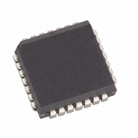
IC LIU T3/E3/STS-1 28-PLCC
Manufacturer
Maxim Integrated Products
Type
Line Interface Units (LIUs)r
Datasheet
1.DS3150T.pdf
(28 pages)
Specifications of DS3150Q+
Number Of Drivers/receivers
1/1
Protocol
DS3
Voltage - Supply
3.135 V ~ 3.465 V
Mounting Type
Surface Mount
Package / Case
28-LCC, 28-PLCC
Lead Free Status / RoHS Status
Lead free / RoHS Compliant


DS3150
1.2 Transmitter
Transmit Clock. The clock applied at the TCLK input is used to clock in data on the TPOS/TNRZ and
TNEG pins. If the jitter attenuator is not enabled in the transmit path, the signal on TCLK is the transmit
line clock and must be transmission quality (i.e., ±20ppm frequency accuracy and low jitter). If the jitter
attenuator is enabled in the transmit path, the signal on TCLK can be jittery and/or periodically gapped
(not exceeding 8 UI) but must still have an average frequency within ±20ppm of the nominal line rate.
When enabled in the transmit path, the jitter attenuator generates the transmit line clock from the signal
applied on the MCLK pin. The signal on MCLK must, therefore, be a transmission-quality clock
(±20ppm frequency accuracy and low jitter). The duty cycle of TCLK is not restricted as long as the high
and low times listed in Section
3
are met.
To support a glueless interface to a variety of neighboring components, the polarity of TCLK can be
inverted using the ICE input pin. See the ICE pin description in
Table 2-A
for details.
Framer Interface Format and the B3ZS/HDB3 Encoder. Data to be transmitted can be input in
either NRZ or bipolar format. To select the bipolar format, wire the ZCSE input pin high. In this format,
the B3ZS/HDB3 encoder is disabled, and the data to be transmitted is sampled on the TPOS and TNEG
input pins. Positive-polarity pulses are indicated by TPOS = 1 while negative-polarity pulses are indicated
by TNEG = 1. TPOS and TNEG should not be active at the same time.
To select the NRZ format, wire ZCSE low. In this format, the B3ZS/HDB3 encoder is enabled, and the
data to be transmitted is sampled on the TNRZ pin. The TNEG pin is ignored in NRZ mode and should
be tied low.
Pattern Generation. The transmitter can generate a number of different patterns internally, including
unframed all ones (E3 AIS), 1010…, and DS3 AIS. See
Figure 1-5
for the structure of the DS3 AIS
signal. The TDS0 and TDS1 inputs are used to select these on-board patterns.
Table 2-B
indicates the
possible selections.
Waveshaping, Line Build-Out, Line Driver. The waveshaping block converts the transmit clock,
positive data, and negative data signals into a single AMI signal that meets applicable
telecommunications standards when transmitted on 75W coaxial cable.
Table 1-C
through
Table 1-G
and
Figure 1-4
show the waveform template specifications and test parameters from ANSI T1.102, Telcordia
GR-253-CORE and GR-499-CORE, and ITU-T G.703.
Because DS3 and STS-1 signals must meet the waveform templates at the cross-connect through any
cable length from 0 to 450 feet, the waveshaping circuitry includes a selectable LBO feature. For cable
lengths of 225 feet or greater, the LBO pin should be low. When LBO is low, output pulses are driven
onto the coaxial cable without any preattenuation. For cable lengths less than 225 feet, LBO should be
high. When LBO is high, pulses are preattenuated before being driven onto the coaxial cable. The LBO
circuitry provides attenuation that mimics the attenuation of 225 feet of coaxial cable.
To power down the transmitter and tri-state the TX+ and TX- output pins, pull the TTS input pin low.
Interfacing to the Line. The transmitter interfaces to the outgoing DS3/E3/STS-1 coaxial cable (75W)
through a 2:1 step-down transformer connected to the TX+ and TX- output pins.
Figure 1-2
shows the
arrangement of the transformer and other recommended interface components.
10 of 28
Related parts for DS3150Q+
Image
Part Number
Description
Manufacturer
Datasheet
Request
R

Part Number:
Description:
3.3V T3 / E3 / STS-1 Line Interface Unit
Manufacturer:
Maxim Integrated Products
Datasheet:
Part Number:
Description:
MAX7528KCWPMaxim Integrated Products [CMOS Dual 8-Bit Buffered Multiplying DACs]
Manufacturer:
Maxim Integrated Products
Datasheet:
Part Number:
Description:
Single +5V, fully integrated, 1.25Gbps laser diode driver.
Manufacturer:
Maxim Integrated Products
Datasheet:
Part Number:
Description:
Single +5V, fully integrated, 155Mbps laser diode driver.
Manufacturer:
Maxim Integrated Products
Datasheet:
Part Number:
Description:
VRD11/VRD10, K8 Rev F 2/3/4-Phase PWM Controllers with Integrated Dual MOSFET Drivers
Manufacturer:
Maxim Integrated Products
Datasheet:
Part Number:
Description:
Highly Integrated Level 2 SMBus Battery Chargers
Manufacturer:
Maxim Integrated Products
Datasheet:
Part Number:
Description:
Current Monitor and Accumulator with Integrated Sense Resistor; ; Temperature Range: -40°C to +85°C
Manufacturer:
Maxim Integrated Products
Part Number:
Description:
TSSOP 14/A�/RS-485 Transceivers with Integrated 100O/120O Termination Resis
Manufacturer:
Maxim Integrated Products
Part Number:
Description:
TSSOP 14/A�/RS-485 Transceivers with Integrated 100O/120O Termination Resis
Manufacturer:
Maxim Integrated Products
Part Number:
Description:
QFN 16/A�/AC-DC and DC-DC Peak-Current-Mode Converters with Integrated Step
Manufacturer:
Maxim Integrated Products
Part Number:
Description:
TDFN/A/65V, 1A, 600KHZ, SYNCHRONOUS STEP-DOWN REGULATOR WITH INTEGRATED SWI
Manufacturer:
Maxim Integrated Products
Part Number:
Description:
Integrated Temperature Controller f
Manufacturer:
Maxim Integrated Products
Part Number:
Description:
SOT23-6/I�/45MHz to 650MHz, Integrated IF VCOs with Differential Output
Manufacturer:
Maxim Integrated Products
Part Number:
Description:
SOT23-6/I�/45MHz to 650MHz, Integrated IF VCOs with Differential Output
Manufacturer:
Maxim Integrated Products
Part Number:
Description:
EVALUATION KIT/2.4GHZ TO 2.5GHZ 802.11G/B RF TRANSCEIVER WITH INTEGRATED PA
Manufacturer:
Maxim Integrated Products