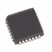
DS3150Q+ Maxim Integrated Products, DS3150Q+ Datasheet - Page 18

DS3150Q+
Manufacturer Part Number
DS3150Q+
Description
IC LIU T3/E3/STS-1 28-PLCC
Manufacturer
Maxim Integrated Products
Type
Line Interface Units (LIUs)r
Datasheet
1.DS3150T.pdf
(28 pages)
Specifications of DS3150Q+
Number Of Drivers/receivers
1/1
Protocol
DS3
Voltage - Supply
3.135 V ~ 3.465 V
Mounting Type
Surface Mount
Package / Case
28-LCC, 28-PLCC
Lead Free Status / RoHS Status
Lead free / RoHS Compliant
NAME
RMON
RNEG/
RPOS/
RCLK
RLCV
RNRZ
TCLK
PRBS
TDS0
RX+,
RX-
(Note 3)
(Note 2)
(Note 2)
TYPE
O3
I3
I3
O
O
O
I
I
PRBS Detector. The PRBS pin reports the status of the PRBS detector. The PRBS
detector constantly searches for either a 2
pseudorandom bit sequence. When the PRBS detector is out of synchronization, the
PRBS pin is driven high. When the detector synchronizes to an incoming PRBS pattern,
the PRBS pin is driven low and then pulses high, synchronous with RCLK, for each bit
error detected. See
is tri-stated. The PRBS pin is only available in the TQFP package type.
Receive Clock. The recovered clock is output on the RCLK pin. The recovered data is
updated at the RPOS/RNRZ and RNEG/RLCV outputs on either the falling edge of
RCLK (ICE = 0 or 1) or the rising edge of RCLK (ICE = FLOAT). During loss of
signal (LOS = 0), the RCLK output signal is derived from the device’s master clock.
Receive Monitor Mode. RMON determines whether or not the receiver’s preamp is
enabled to provide flat to the incoming signal before it is processed by the equalizer.
This feature should be enabled when the device is being used to monitor signals that
have been resistively attenuated by a monitor jack.
This input also controls the jitter attenuator
0 = disable the monitor preamp, disable the jitter attenuator in the receive path
1 = enable the monitor preamp, disable the jitter attenuator in the receive path
Float = disable the monitor preamp, enable the jitter attenuator in the receive path
Receive Negative Data or Receive Line Code Violation. When the B3ZS/HDB3
decoder is disabled (ZCSE = 1), RNEG pulses high to indicate reception of a negative
AMI pulse. When the B3ZS/HDB3 decoder is enabled (ZCSE = 0), the NRZ data
stream is output on RNRZ while RLCV is pulsed high for one RCLK period whenever
the decoder sees a line coding violation. RNEG/RLCV is updated either on the rising
edge of RCLK (ICE = Float) or the falling edge of RCLK (ICE = 0 or 1).
Receive Positive Data or Receive NRZ Data. When the B3ZS/HDB3 decoder is
disabled (ZCSE = 1), RPOS pulses high to indicate reception of a positive AMI pulse.
When the B3ZS/HDB3 decoder is enabled (ZCSE = 0), the NRZ data stream is output
on RNRZ while RLCV is pulsed high whenever the decoder sees a line coding
violation. RPOS/RNRZ is updated either on the rising edge of RCLK (ICE = Float) or
the falling edge of RCLK (ICE = 0 or 1).
Receive Analog Inputs. These differential AMI inputs are coupled to the inbound 75W
coaxial cable through a 1:2 step-up transformer
Transmit Clock. A DS3 (44.736MHz), E3 (34.368MHz), or STS-1 (51.840MHz) clock
should be applied to the TCLK pin. Data to be transmitted is clocked into the device at
TPOS/TNRZ and TNEG either on the rising edge of TCLK (ICE = 0) or the falling
edge of TCLK (ICE = 1 or FLOAT). The duty cycle on TCLK is not restricted as long
the high and low times listed in Section
Transmit Data Select Bit 0. If EFE = 1, TDS0, TDS1 and TESS select the source of
the transmit data
(Table
Figure 1-6
2-B). If EFE = 0, TDS0 is ignored.
18 of 28
and
Figure 1-7
FUNCTION
3
15
are met. See Section
- 1 (DS3 or STS-1) or 2
(Table
for more details. If EFE = 0, the PRBS pin
(Figure
2-C).
1-2).
1.3
for additional details
23
- 1 (E3)


