74LVXC4245WM Fairchild Semiconductor, 74LVXC4245WM Datasheet

TXRX 8BIT DUAL CONF VOLT 24SOIC

74LVXC4245WM

Manufacturer Part Number
74LVXC4245WM
Description
TXRX 8BIT DUAL CONF VOLT 24SOIC
Manufacturer
Fairchild Semiconductor
Series
74LVr
Type
Transceiverr
Datasheets

Specifications of 74LVXC4245WM

Number Of Drivers/receivers
8/8
Voltage - Supply
2.7 V ~ 5.5 V
Mounting Type
Surface Mount
Package / Case
24-SOIC (7.5mm Width)
Logic Family
LVX
Operating Supply Voltage (typ)
3.3/5/5V
Propagation Delay Time
11ns
Number Of Elements
1
Number Of Channels
8
Input Logic Level
CMOS
Output Logic Level
CMOS
Output Type
3-State
Package Type
SOIC W
Polarity
Non-Inverting
Operating Supply Voltage (min)
2.7/4.5V
Operating Supply Voltage (max)
5.5V
Technology
CMOS
Operating Temp Range
-40C to 85C
Operating Temperature Classification
Industrial
Mounting
Surface Mount
Additional Features
W/Volt Translation
Pin Count
24
Logic Device Type
Transceiver, Non Inverting
Supply Voltage Range
4.5V To 5.5V
Logic Case Style
SOIC
No. Of Pins
24
Operating Temperature Range
-40°C To +85°C
Svhc
No SVHC (15-Dec-2010)
Rohs Compliant
Yes
Lead Free Status / RoHS Status
Lead free / RoHS Compliant
Protocol
-
Lead Free Status / Rohs Status
Compliant

Available stocks

Company
Part Number
Manufacturer
Quantity
Price
Part Number:
74LVXC4245WMX
Manufacturer:
FAIRCHILD/仙童
Quantity:
20 000
© 2003 Fairchild Semiconductor Corporation
74LVXC4245WM
74LVXC4245QSC
74LVXC4245MTC
74LVXC4245
8-Bit Dual Supply Configurable Voltage Interface
Transceiver with 3-STATE Outputs
General Description
The LVXC4245 is a 24-pin dual-supply, 8-bit configurable
voltage interface transceiver suited for PCMCIA and other
real time configurable I/O applications. The V
accepts a 5V supply level. The “A” Port is a dedicated 5V
port. The V
“B” Port is configured to track the V
respectively. A 5V level on the V
I/O pins at a 5V level and a 3V V
pins at a 3V level. This device will allow the V
source pin and I/O pins on the “B” Port to float when OE is
HIGH. This feature is necessary to buffer data to and from
a PCMCIA socket that permits PCMCIA cards to be
inserted and removed during normal operation.
Ordering Code:
Devices also available in Tape and Reel. Specify by appending the suffix letter “X” to the ordering code.
Logic Symbol
Pin Descriptions
Order Number
Pin Names
A
B
T/R
OE
0
0
–A
–B
7
7
CCB
pin accepts a 3V-to-5V supply level. The
Output Enable Input
Transmit/Receive Input
Side A Inputs or 3-STATE Outputs
Side B Inputs or 3-STATE Outputs
Package Number
MQA24
MTC24
M24B
Description
CC
CC
pin will configure the
will configure the I/O
24-Lead Small Outline Integrated Circuit (SOIC), JEDEC MS-013, 0.300" Wide
24-Lead Quarter Size Outline Package (QSOP), JEDEC MO-137, 0.150" Wide
24-Lead Thin Shrink Small Outline Package (TSSOP), JEDEC MO-153, 4.4mm Wide
CCB
supply level
CCB
DS012009
CCA
voltage
pin
Features
Connection Diagram
Bidirectional interface between 5V and 3V-to-5V buses
Control inputs compatible with TTL level
Outputs source/sink up to 24 mA
Guaranteed simultaneous switching noise level and
dynamic threshold performance
Implements patented EMI reduction circuitry
Flexible V
Allows B Port and V
is HIGH
Functionally compatible with the 74 series 245
Package Description
CCB
operating range
CCB
to float simultaneously when OE
February 1994
Revised October 2003
www.fairchildsemi.com

Related parts for 74LVXC4245WM

74LVXC4245WM Summary of contents

Page 1

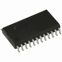
... PCMCIA socket that permits PCMCIA cards to be inserted and removed during normal operation. Ordering Code: Order Number Package Number 74LVXC4245WM M24B 24-Lead Small Outline Integrated Circuit (SOIC), JEDEC MS-013, 0.300" Wide 74LVXC4245QSC MQA24 24-Lead Quarter Size Outline Package (QSOP), JEDEC MO-137, 0.150" Wide ...

Page 2

Truth Table HIGH Voltage Level L LOW Voltage Level X Immaterial Logic Diagram www.fairchildsemi.com Inputs Outputs T/R L Bus B Data to Bus A H Bus A Data to Bus B X HIGH-Z State 2 ...

Page 3

Absolute Maximum Ratings Supply Voltage ( CCA CCB DC Input Voltage ( OE, T/R 0. Input/Output Voltage ( ...

Page 4

DC Electrical Characteristics V CCA Symbol Parameter (V) I Maximum 3-STATE 5.5 OZA Output Leakage @ A 5 Maximum 3-STATE 5.5 OZB Output Leakage @ B 5 Maximum All Inputs 5 /Input B 5.5 ...

Page 5

AC Electrical Characteristics V CCA V CCB Symbol Parameter Min Typ (Note 6) t Propagation 1.0 4.9 PHL t Delay 1.0 4.0 PLH t Propagation 1.0 4.7 PHL t Delay ...

Page 6

Configurable I/O Application for PCMCIA Cards The LVXC4245 is a 24-pin dual supply device well suited for PCMCIA configurable I/O applications. Ideal for low power notebook designs, the LVXC4245 consumes less than quiescent power in all modes ...

Page 7

Physical Dimensions inches (millimeters) unless otherwise noted 24-Lead Small Outline Integrated Circuit (SOIC), JEDEC MS-013, 0.300" Wide 24-Lead Quarter Size Outline Package (QSOP), JEDEC MO-137, 0.150" Wide Package Number M24B Package Number MQA24 7 www.fairchildsemi.com ...

Page 8

Physical Dimensions inches (millimeters) unless otherwise noted (Continued) 24-Lead Thin Shrink Small Outline Package (TSSOP), JEDEC MO-153, 4.4mm Wide Fairchild does not assume any responsibility for use of any circuitry described, no circuit patent licenses are implied and Fairchild reserves ...

Related keywords