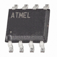
ATA6625-TAPY 19 Atmel, ATA6625-TAPY 19 Datasheet - Page 17

ATA6625-TAPY 19
Manufacturer Part Number
ATA6625-TAPY 19
Description
TXRX LIN BUS 5V W/VREG 8SOIC
Manufacturer
Atmel
Type
Transceiverr
Datasheet
1.ATA6623C-TAPY.pdf
(23 pages)
Specifications of ATA6625-TAPY 19
Number Of Drivers/receivers
1/1
Protocol
LIN
Voltage - Supply
5 V ~ 27 V
Mounting Type
Surface Mount
Package / Case
SO-8
Lead Free Status / RoHS Status
Lead free / RoHS Compliant
9. Electrical Characteristics (Continued)
5V < V
4957I–AUTO–03/11
*) Type means: A = 100% tested, B = 100% correlation tested, C = Characterized on samples, D = Design parameter
8.10
8.11
8.12
8.13
10.1
10.2
10.3
10.4
No.
8.9
9.1
9.2
9.3
9.4
9.5
9.6
10
9
S
< 27V, –40°C < T
Parameters
Input leakage current at
the receiver including
pull-up resistor as
specified
Leakage current LIN
recessive
Leakage current when
control unit disconnected
from ground. Loss of
local ground must not
affect communication in
the residual network
Leakage current at
disconnected battery.
Node has to sustain the
current that can flow
under this condition. Bus
must remain operational
under this condition.
Capacitance on Pin LIN
to GND
LIN Bus Receiver
Center of receiver
threshold
Receiver dominant state V
Receiver recessive state V
Receiver input
hysteresis
Pre-wake detection LIN
High level input voltage
Pre-wake detection LIN
Low level input voltage
Internal Timers
Dominant time for
wake–up via LIN bus
Time delay for mode
change from Fail-safe
into Normal Mode via pin
EN
Time delay for mode
change from Normal
Mode to Sleep Mode via
pin EN
TXD dominant time out
time
j
< 150°C; unless otherwise specified all values refer to GND pins.
Test Conditions
Input Leakage current
Driver off
V
V
Driver off
8V < V
8V < V
V
GND
V
0V < V
V
V
0V < V
V
(V
V
Activates the LIN receiver
V
V
V
V
BUS
Batt
BUS
Batt
Batt
SUP_Device
BUS_CNT
EN
EN
hys
LIN
EN
EN
TXD
th_dom
= 5V
= 5V
= V
= 5V
= 0V
= 0V
= 12V
= 12V
Device
disconnected
= 0V
= 0V
Batt
BUS
BUS
BUS
V
th_rec
+ V
Batt
=
< 18V
< 18V
= V
< 18V
< 18V
= GND
th_rec
– V
S
)/2
th_dom
TXD
Pin
LIN
LIN
LIN
LIN
LIN
LIN
LIN
LIN
LIN
LIN
LIN
LIN
EN
EN
I
I
I
BUS_PAS_dom
I
BUS_PAS_rec
BUS_NO_gnd
BUS_NO_bat
V
Symbol
V
V
V
BUS_CNT
V
BUSdom
V
t
C
BUShys
t
BUSrec
t
t
sleep
norm
dom
LINH
LINL
bus
LIN
Atmel ATA6623/ATA6625
0.6
0.475
0.028
V
S
Min.
–10
–27
–27
V
V
–1
30
– 2V
5
2
6
S
S
V
S
0.1 x V
–0.35
0.5
Typ.
+0.5
0.1
10
V
90
13
7
S
S
V
0.4
0.525
0.175
S
Max.
V
0.3V
+10
150
– 3.3V
20
20
V
40
V
20
15
20
S
2
S
S
+
V
S
Unit
mA
ms
µA
µA
µA
pF
µs
µs
µs
V
V
V
V
V
V
Type*
D
A
A
A
A
A
A
A
A
A
A
A
A
A
A
17


