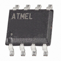
ATA6625-TAPY 19 Atmel, ATA6625-TAPY 19 Datasheet - Page 4

ATA6625-TAPY 19
Manufacturer Part Number
ATA6625-TAPY 19
Description
TXRX LIN BUS 5V W/VREG 8SOIC
Manufacturer
Atmel
Type
Transceiverr
Datasheet
1.ATA6623C-TAPY.pdf
(23 pages)
Specifications of ATA6625-TAPY 19
Number Of Drivers/receivers
1/1
Protocol
LIN
Voltage - Supply
5 V ~ 27 V
Mounting Type
Surface Mount
Package / Case
SO-8
Lead Free Status / RoHS Status
Lead free / RoHS Compliant
3.7
3.8
3.9
3.10
4
Input Pin (TXD)
Dominant Time-out Function (TXD)
Output Pin (RXD)
Enable Input Pin (EN)
Atmel ATA6623/ATA6625
In Normal Mode the TXD pin is the microcontroller interface to control the state of the LIN out-
put. TXD must be pulled to ground in order to drive the LIN bus low. If TXD is high or
unconnected (internal pull-up resistor), the LIN output transistor is turned off and the bus is in
the recessive state.
The TXD input has an internal pull-up resistor. An internal timer prevents the bus line from
being driven permanently in the dominant state. If TXD is forced to low longer than t
the LIN bus driver is switched to the recessive state.
To reactivate the LIN bus driver, switch TXD to high (> 10µs).
This output pin reports the state of the LIN-bus to the microcontroller. LIN high (recessive
state) is reported by a high level at RXD; LIN low (dominant state) is reported by a low level at
RXD. The output has an internal pull-up resistor with typically 5k to V
tics are measured with an external load capacitor of 20pF.
The output is short-circuit protected. In Unpowered Mode (that is, V
off.
The Enable Input pin controls the operation mode of the device. If EN is high, the circuit is in
Normal Mode, with transmission paths from TXD to LIN and from LIN to RXD both active. The
VCC voltage regulator operates with 3.3V/5V/85mA output capability.
If EN is switched to low while TXD is still high, the device is forced to Silent Mode. No data
transmission is then possible, and the current consumption is reduced to I
VCC regulator has its full functionality.
If EN is switched to low while TXD is low, the device is forced to Sleep Mode. No data trans-
mission is possible, and the voltage regulator is switched off.
S
CC
= 0V), RXD is switched
. The AC characteris-
VS
typ. 57µA. The
4957I–AUTO–03/11
dom
> 6ms,


