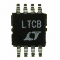
LTC1482CMS8 Linear Technology, LTC1482CMS8 Datasheet - Page 12

LTC1482CMS8
Manufacturer Part Number
LTC1482CMS8
Description
IC TXRX RS485 LOWPWR 8-MSOP
Manufacturer
Linear Technology
Type
Transceiverr
Datasheet
1.LTC1482CN8.pdf
(16 pages)
Specifications of LTC1482CMS8
Number Of Drivers/receivers
1/1
Protocol
RS422, RS485
Voltage - Supply
4.75 V ~ 5.25 V
Mounting Type
Surface Mount
Package / Case
8-MSOP, Micro8™, 8-uMAX, 8-uSOP,
Lead Free Status / RoHS Status
Contains lead / RoHS non-compliant
Available stocks
Company
Part Number
Manufacturer
Quantity
Price
Company:
Part Number:
LTC1482CMS8
Manufacturer:
LT
Quantity:
10 000
Part Number:
LTC1482CMS8
Manufacturer:
LINEAR/凌特
Quantity:
20 000
Company:
Part Number:
LTC1482CMS8#PBF
Manufacturer:
Linear Technology
Quantity:
135
Part Number:
LTC1482CMS8#PBF
Manufacturer:
LINEAR/凌特
Quantity:
20 000
Part Number:
LTC1482CMS8#TRPBF
Manufacturer:
LINEAR/凌特
Quantity:
20 000
APPLICATIONS
LTC1482
Carrier Detect Operation
The carrier detect or CD pin is an open-drain output with
a weak internal pull-up (30 A typical). This allows several
LTC1482s to share the same carrier detect line. The
internal pull-up has a series diode, permitting users to tie
the CD output to a voltage higher than V
driving low, the CD output can sink up to 4mA while
maintaining the output below a TTL V
external pull-up resistor is recommended if fast rise times
are important.
The LTC1482 defines the presence of a carrier as
V
carrier is present. When the carrier is absent, the weak
internal pull-up pulls CD high. For slow moving input
signals (below about 32kHz for signals conforming to
RS485 specifications), the CD output will go high when the
(A – B) signal is within the V
For faster input signals, the CD output does not glitch high
when the (A – B) signal is traversing the transition region.
This is achieved through internal delays in the CD signal
path. It takes t
signal is removed. There are no additional built-in delays
for CD going low so that t
When the LTC1482 is not in shutdown mode, CD = 1
always forces the receiver output (RO) high. If the driver
is enabled (DE = 1), CD = 0 as long as V
excessive loading between these pins will cause this
condition to be violated and the CD pin will pull high. If the
driver is disabled, CD is guaranteed to go high when:
The last condition occurs if the external driver is loaded
excessively.
In shutdown mode, RO is three-stated and CD is taken high
by the weak internal pull-up. On exiting shutdown, it takes
longer (t
carrier is present.
12
THCD(MIN)
V
a) A is shorted to B,
b) A and B are open (with or without termination) or
c) V
THCD
THCD
CDL(SHDN)
max. Shorting the A and B pins together or
min A – B V
CDH
(A – B) V
( 5 s) for CD to go high after the carrier
= 5 s max) for CD to pull low when a
U
INFORMATION
THCD(MAX)
U
CDL
THCD(MIN)
THCD
is only 300ns max.
max
. CD pulls low when a
W
to V
CC
THCD
THCD(MAX)
(8V max). When
OL
min (A – B)
of 0.4V. An
U
range.
When V
to become valid. The time needed depends on the capaci-
tance at the CD pin, the V
connected to the A and B pins. For a load capacitance of
15pF and a 1 s V
recommended.
Receiver Output and Fail-Safe
If CD is low, the receiver output, RO, responds to the input
differential voltage and is guaranteed (by testing) to go
high if (A – B) V
Some data encoding schemes require that the output of
the receiver maintain a known state (usually logic 1) when
data transmission ends and all drivers on the line are
forced into three-state. The carrier detect mechanism
ensures that RO will be high regardless of whether the line
is open, floating or shorted together, or whether the line is
terminated or not. This removes external components
required with earlier RS485 devices for the case where the
required known state is a logic 1. External components are
needed if the required state is a logic 0.
Fail-safe operates over the – 7V to 12V common mode
range and fast common mode steps do not affect the
receiver output.
Note that the CD output only goes high after all the drivers
are three-stated due to built-in delays (t
signal path (see Carrier Detect Operation). During the time
interval (see Figure 11) beginning at driver three-state and
ending at CD going high, the receiver output stays at the
last state just prior to the driver three-stating.
I
The supply current of the LTC1482 is reduced to 20 A max
by taking both the DE and DI/SHDN pins low. In shutdown,
all internal circuits are powered down and the driver and
receiver outputs are three-stated. The CD output is taken
high by the weak internal pull-up.
Logic within the LTC1482 prevents slow DE and DI/SHDN
transitions from generating internal shutdown pulses by
rejecting “shutdown pulses” of less than 50ns (typ) in
duration. Without this logic, the driver outputs will glitch
when three-stated momentarily.
CC
Shutdown Mode
CC
is applied, some time is needed for CD and RO
THRO(MAX)
CC
rise time, a wait time of 10 s is
and low if (A – B) V
CC
rise time and the loads
CDH
) in the CD
THCD(MIN)
.


