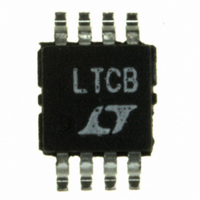
LTC1482CMS8 Linear Technology, LTC1482CMS8 Datasheet - Page 3

LTC1482CMS8
Manufacturer Part Number
LTC1482CMS8
Description
IC TXRX RS485 LOWPWR 8-MSOP
Manufacturer
Linear Technology
Type
Transceiverr
Datasheet
1.LTC1482CN8.pdf
(16 pages)
Specifications of LTC1482CMS8
Number Of Drivers/receivers
1/1
Protocol
RS422, RS485
Voltage - Supply
4.75 V ~ 5.25 V
Mounting Type
Surface Mount
Package / Case
8-MSOP, Micro8™, 8-uMAX, 8-uSOP,
Lead Free Status / RoHS Status
Contains lead / RoHS non-compliant
Available stocks
Company
Part Number
Manufacturer
Quantity
Price
Company:
Part Number:
LTC1482CMS8
Manufacturer:
LT
Quantity:
10 000
Part Number:
LTC1482CMS8
Manufacturer:
LINEAR/凌特
Quantity:
20 000
Company:
Part Number:
LTC1482CMS8#PBF
Manufacturer:
Linear Technology
Quantity:
135
Part Number:
LTC1482CMS8#PBF
Manufacturer:
LINEAR/凌特
Quantity:
20 000
Part Number:
LTC1482CMS8#TRPBF
Manufacturer:
LINEAR/凌特
Quantity:
20 000
SWITCHING CHARACTERISTICS
temperature range, otherwise specifications are at T
SYMBOL
V
V
V
I
R
I
I
I
I
I
I
temperature range, otherwise specifications are at T
SYMBOL
t
t
t
t
t
t
t
t
t
t
t
t
f
t
t
t
t
t
ELECTRICAL CHARACTERISTICS
OZR
CC
SHDN
OSD1
OSD2
OS
PULL-UP
PLH
PHL
SKEW
r
ZH
ZL
LZ
HZ
ZH(SHDN)
ZL(SHDN)
HZ(SHDN)
LZ(SHDN)
MAX
PLH
PHL
SKD
CDH
CDL
THCD
OH
OL
, t
V
IN
TH
f
PARAMETER
Differential Input Threshold Voltage for CD = 1
Receiver Input Hysteresis
CD Output High Voltage
RO Output High Voltage
RO and CD Output Low Voltage
Three-State (High Impedance) Receiver Output
Current in Shutdown
Receiver Input Resistance
Supply Current
Supply Current in Shutdown Mode
Driver Short-Circuit Current, V
Driver Short-Circuit Current, V
RO and CD Short-Circuit Current
CD Pull-Up Current
PARAMETER
Driver Input to Output
Driver Input to Output
Driver Output to Output
Driver Rise or Fall Time
Driver Enable to Output High
Driver Enable to Output Low
Driver Disable Time from Low
Driver Disable Time from High
Driver Enable from Shutdown to Output High
(Note 5)
Driver Enable from Shutdown to Output Low
Driver Disable on Shutdown from Output High
Driver Disable on Shutdown from Output Low
Maximum Data Rate (Note 6)
Receiver Input to Output (Note 7)
Receiver Input to Output
|t
Receiver Input to CD Output High (Note 7)
Receiver Input to CD Output Low (Note 7)
PLH
U
– t
PHL
| Differential Receiver Skew
OUT
OUT
= High (Note 4)
= Low (Note 4)
A
A
= 25 C. V
= 25 C. V
CONDITIONS
– 7V V
V
I
I
I
V
DI/SHDN = 0, DE = 0
–7V V
No Load, Driver Enabled (DE = V
No Load, Driver Disabled (DE = 0)
DE = 0, DI = 0
– 7V V
– 7V V
0V V
CD = 0V
CONDITIONS
R
(Figures 4, 6)
C
C
C
C
C
C
C
C
R
(Figures 4, 8)
R
(Figures 4, 8)
R
(Figures 4, 8)
R
(Figures 4, 10) DI/SHDN = V
R
(Figures 4, 10) DI/SHDN = V
OUT
OUT
OUT
The
CM
CC
The
DIFF
L
L
L
L
L
L
L
L
DIFF
DIFF
DIFF
DIFF
DIFF
= 100pF (Figures 5, 7) S2 Closed
= 100pF (Figures 5, 7) S1 Closed
= 15pF (Figures 5, 7) S1 Closed
= 15pF (Figures 5, 7) S2 Closed
= 100pF (Figures 5, 7) S2 Closed
= 100pF (Figures 5, 7) S1 Closed
= 15pF (Figures 5, 7) S2 Closed
= 15pF (Figures 5, 7) S1 Closed
= Max, 0.4V V
= 0V, DE = 0
= – 10 A, (V
= – 4mA, (V
= 4mA, (V
= 54 , C
= 54 , C
= 54 , C
= 54 , C
= 54 , C
= 54 , C
OUT
CC
CC
CM
CM
OUT
OUT
denotes the specifications which apply over the full operating
denotes the specifications which apply over the full operating
= 5V 5% (Notes 2 and 3) unless otherwise noted.
= 5V 5% (Notes 2 and 3) unless otherwise noted.
V
12V, DE = 0
12V
CC
10V
10V
A
L1
L1
L1
L1
L1
L1
A
– V
A
= C
= C
= C
= C
= C
= C
– V
– V
B
OUT
L2
L2
L2
L2
L2
L2
) = – 200mV
B
B
) = 200mV
) = 0V
= 100pF
= 100pF,
= 100pF,
= 100pF,
= 100pF,
= 100pF,
2.4V
CC
CC
CC
)
– 0.20
MIN
MIN
3.4
3.5
12
35
35
15
10
10
30
30
7
3
4
2900
TYP
580
430
TYP
138
122
150
22
10
30
28
30
15
40
40
40
40
40
40
40
40
16
2
5
30
LTC1482
5000
MAX
MAX
0.20
900
700
250
250
100
100
100
100
100
200
200
300
0.4
20
85
60
60
60
10
40
70
70
70
1
UNITS
UNITS
Mbps
3
mV
mA
mA
mA
k
ns
ns
ns
ns
ns
ns
ns
ns
ns
ns
ns
ns
ns
ns
ns
ns
ns
V
V
V
V
A
A
A
A
A


