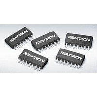
FM3204-G Ramtron, FM3204-G Datasheet - Page 16

FM3204-G
Manufacturer Part Number
FM3204-G
Description
Supervisory Circuits 4K w/Pwr Mon WDT Bat Sw Pwr Fail
Manufacturer
Ramtron
Datasheet
1.FM3264-G.pdf
(21 pages)
Specifications of FM3204-G
Number Of Voltages Monitored
4
Monitored Voltage
2.6 V or 2.9 V or 3.9 V or 4.4 V
Output Type
Active Low or Bidirectional
Manual Reset
Resettable
Watchdog
Watchdog
Battery Backup Switching
Backup
Power-up Reset Delay (typ)
200 ms
Supply Voltage (max)
5.5 V
Supply Voltage (min)
2.7 V
Supply Current (typ)
1500 uA
Maximum Operating Temperature
+ 85 C
Mounting Style
SMD/SMT
Package / Case
SOIC-14
Minimum Operating Temperature
- 40 C
Power Fail Detection
Yes
Lead Free Status / Rohs Status
Lead free / RoHS Compliant
Electrical Specifications
Absolute Maximum Ratings
* PFI input voltage must not exceed 4.5V.
** The “V
Stresses above those listed under Absolute Maximum Ratings may cause permanent damage to the device. This is a stress rating only,
and the functional operation of the device at these or any other conditions above those listed in the operational section of this
specification is not implied. Exposure to absolute maximum ratings conditions for extended periods may affect device reliability.
DC Operating Conditions (
Rev. 3.1
July 2010
Symbol
V
I
I
V
I
I
V
V
V
V
V
I
I
V
V
V
V
R
DD
SB
BAK
BAKTC
LI
LO
RST
DD
BAK
TP0
TP1
TP2
TP3
RST
IL
IH
OL
OH
Symbol
T
V
V
T
V
V
LEAD
IN
BAK
STG
ESD
DD
IN
< V
Main Power Supply
V
Standby Current
Backup Supply Voltage
Backup Supply Current
Trickle Charge Current
V
V
V
V
V
Input Leakage Current
Output Leakage Current
Input Low Voltage
Input High Voltage
Output Low Voltage (I
Output High Voltage (I
Pull-up resistance for /RST inactive
DD
@
@
@
For V
For V
DD
DD
DD
DD
DD
DD
V
V
All inputs except those listed below
CNT1-2 battery backed (V
All inputs except those listed below
PFI (comparator input)
CNT1-2 battery backed (V
CNT1-2 (V
CNT1-2 V
+1.0V” restriction does not apply to the SCL and SDA inputs which do not employ a diode to V
BAK
BAK
SCL = 100 kHz
SCL = 400 kHz
SCL = 1 MHz
Supply Current
Trip Point Voltage, VTP(1:0) = 00b
Trip Point Voltage, VTP(1:0) = 01b
Trip Point Voltage, VTP(1:0) = 10b
Trip Point Voltage, VTP(1:0) = 11b
for valid /RST
DD
DD
> V
< V
Power Supply Voltage with respect to V
Voltage on any signal pin with respect to V
Backup Supply Voltage
Storage Temperature
Lead Temperature (Soldering, 10 seconds)
Electrostatic Discharge Voltage
Package Moisture Sensitivity Level
- Human Body Model
- Charged Device Model
- Machine Model (JEDEC Std JESD22-A115-A)
< 5.5V
< 3.6V
BAK
BAK
DD
DD
min
min
> 2.5V
T
> 2.5V)
Parameter
A
= -40° C to + 85° C, V
@
I
OL
OL
OH
= 3 mA)
= 80 µA at V
= -2 mA)
Description
DD
DD
< 2.5V)
< 2.5V)
(JEDEC Std JESD22-A114-B)
(JEDEC Std JESD22-C101-A)
OL
DD
= 2.7V to 5.5V unless otherwise specified)
SS
V
0.7 V
0.7 V
BAK
SS
Min
2.55
2.85
3.80
4.25
-0.3
-0.3
-0.3
2.7
2.0
1.6
2.4
50
5
0
-
-
– 0.5
DD
DD
Typ
3.0
2.6
2.9
3.9
4.4
-1.0V to +7.0V * and
V
-55°C to + 125°C
IN
-1.0V to +7.0V
-1.0V to +4.5V
≤ V
V
V
V
Ratings
0.3 V
MSL-1
BAK
260° C
DD
DD
250V
Max
1500
4kV
1kV
3.75
2.70
3.00
4.00
4.50
3.75
DD
500
900
150
120
400
5.5
0.5
0.8
0.4
±1
±1
25
1
-
+ 0.3
+ 0.3
+1.0V **
DD
+ 0.3
DD
.
FM3204/16/64/256
Units
KΩ
µA
µA
µA
µA
µA
µA
µA
µA
µA
V
V
V
V
V
V
V
V
V
V
V
V
V
V
V
V
V
Page 16 of 21
Notes
10
7
1
2
9
4
6
3
3
8
5
5
5
5


