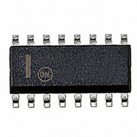
MC26LS30DR2G ON Semiconductor, MC26LS30DR2G Datasheet - Page 10

MC26LS30DR2G
Manufacturer Part Number
MC26LS30DR2G
Description
IC DRIVER LINE CONFIG 16SOIC
Manufacturer
ON Semiconductor
Type
Driverr
Datasheet
1.MC26LS30DG.pdf
(14 pages)
Specifications of MC26LS30DR2G
Number Of Drivers/receivers
4/0
Protocol
RS422, RS423
Voltage - Supply
4.75 V ~ 5.25 V
Mounting Type
Surface Mount
Package / Case
16-SOIC (3.9mm Width)
Lead Free Status / RoHS Status
Lead free / RoHS Compliant
Other names
MC26LS30DR2GOS
MC26LS30DR2GOS
MC26LS30DR2GOSTR
MC26LS30DR2GOS
MC26LS30DR2GOSTR
transients induced onto the drivers’ outputs from the
external cable (from ESD, motor noise, nearby computers,
etc.).
Operating Temperature Range
+85 C, is actually a function of the system use (i.e.,
specifically how many drivers within a package are used)
and at what current levels they are operating. The maximum
power which may be dissipated within the package is
determined by:
where R
1) Differential Mode Power Dissipation
package is calculated from:
where: V
As indicated in the equation, the first term (in brackets) must
be calculated and summed for each of the two drivers, while
the last term is common to the entire package. Note that the
term (V
not vary with V
following conditions:
suitability of the package types is calculated as follows.
P D + [ (V CC * V OD )
The maximum ambient operating temperature, listed as
120 C/W for the SOIC (D) package,
T
T
For the differential mode, the power dissipated within the
T
The power dissipated is:
A
A
Jmax
= +85 C, I
= ambient air temperature near the IC package.
CC
= max. allowable junction temperature (150 C)
V
I
JA
B
CC
OD
−V
= package thermal resistance which is typically:
OD
= the supply voltage
= is taken from Figure 6 for the known
= the internal bias current (Figure 7)
O
) is constant for a given value of I
P Dmax + T Jmax * T A
= −60 mA (each driver), V
value of I
CC
. For an application involving the
I O ] (each driver) ) (V CC
O
R qJA
CC
= 5.25 V, the
O
and does
http://onsemi.com
MC26LS30
I B )
10
exceeded in any of the above cases, either package can be
used in this application.
2) Single−Ended Mode Power Dissipation
the package is calculated from:
for both output states, and makes use of the fact that the
absolute value of the graphs of Figures 10 and 11 are nearly
identical. I
Figures 12 and 13, and (V
Figure 10. Note that the term (V
given value of I
application involving the following conditions:
V
calculated as follows.
exceeded in any of the above cases, either package can be
used in this application.
EE
The junction temperature calculates to:
Since the maximum allowable junction temperature is not
For the single−ended mode, the power dissipated within
The above equation assumes I
T
The power dissipated is:
The junction temperature calculates to:
Since the maximum allowable junction temperature is not
T J + 85°C ) (0.490 W
A
T J + 85°C ) (0.454 W
P D + 490 mW
P D + [ 3.0 V
P D + 454 mW
P D + ( 24 mA
= −5.25 V, the suitability of the package types is
= +85 C, I
SOIC package.
SOIC package.
B
[ ( I O
P D + ( I B)
[ 60 mA
+ and I
O
O
( V CC * V OH ) ] ( each driver )
= −60 mA (each driver), V
B
and does not vary with V
− are obtained from the right half of
60 mA
5.25 V ) ) ( *3.0 mA
1.45 V
CC
V CC ) ) ( I B*
− V
120°C W) + 144°C for the
120°C W) + 139°C for the
2 ] ) (5.25 V
CC
O
4.0 ]
OH
has the same magnitude
− V
) can be obtained from
OH
) is constant for a
V EE ) )
CC
*5.25 V ) )
CC
18 mA)
= 5.25 V,
. For an


