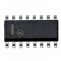
MC26LS30DR2G ON Semiconductor, MC26LS30DR2G Datasheet - Page 3

MC26LS30DR2G
Manufacturer Part Number
MC26LS30DR2G
Description
IC DRIVER LINE CONFIG 16SOIC
Manufacturer
ON Semiconductor
Type
Driverr
Datasheet
1.MC26LS30DG.pdf
(14 pages)
Specifications of MC26LS30DR2G
Number Of Drivers/receivers
4/0
Protocol
RS422, RS423
Voltage - Supply
4.75 V ~ 5.25 V
Mounting Type
Surface Mount
Package / Case
16-SOIC (3.9mm Width)
Lead Free Status / RoHS Status
Lead free / RoHS Compliant
Other names
MC26LS30DR2GOS
MC26LS30DR2GOS
MC26LS30DR2GOSTR
MC26LS30DR2GOS
MC26LS30DR2GOSTR
1. All voltages measured with respect to Pin 5.
2. Only one output shorted at a time, for not more than 1 second.
3. Typical values established at +25 C, V
4. V
5. Imbalance is the difference between V
ELECTRICAL CHARACTERISTICS
V
TIMING CHARACTERISTICS
unless otherwise noted.)
Output Voltage (see Figure 1)
Output Current (each output)
Inputs
Power Supply Current (V
Differential Output Rise Time (Figure 3)
Differential Output Fall Time (Figure 3)
Propagation Delay Time − Input to Differential Output
Skew Timing (Figure 3)
Enable Timing (Figure 4)
EE
Differential, R
Differential, R
Change in Differential Voltage, R
Offset Voltage, R
Change in Offset Voltage*, R
Power Off Leakage, V
High Impedance Mode, V
Short Circuit Current (Note 2)
Low Level Voltage
High Level Voltage
Current @ V
Current @ V
Current @ V
Current, 0 p V
Clamp Voltage (I
(0 p Enable p V
Input Low to High (Figure 3)
Input High to Low (Figure 3)
Max to Min t
Max to Min t
Enable to Active High Differential Output
Enable to Active Low Differential Output
Enable to 3−State Output From Active High
Enable to 3−State Output From Active Low
in
t
= Gnd, unless otherwise noted. Pin numbers refer to SO−16 package only.)
PDH
High Output Shorted to Pin 5 (T
High Output Shorted to Pin 5 (−40 C t T
Low Output Shorted to +6.0 V (T
Low Output Shorted to +6.0 V (−40 C t T
switched from 0.8 to 2.0 V.
to t
PDL
PDH
PDL
in
in
in
L
L
= 2.4 V
= 15 V
= 0.4 V
for Each Driver
in
= , V
= 100 , V
Within a Package
in
Within a Package
L
p 15 V, V
CC
= 100
= −12 mA)
)
CC
CC
CC
= 5.25 V
= 0, −10 V p V
CC
CC
= +5.25 V, Outputs Open)
Characteristic
CC
Characteristic
L
= 5.25 V, −10 V p V
= 4.75 V
= 100
= 0
(EIA−422−A differential mode, Pin 4 p 0.8 V, T
L
A
= 100
A
= 25 C)
= 25 C)
CC
O2
(EIA−422−A differential mode, Pin 4 p 0.8 V, −40 C tT
O
= +5.0 V, V
with V
p +10 V
(Note 4)
A
A
t+85 C)
t +85 C)
in
O
t 0.8 V and V
p +10 V
EE
http://onsemi.com
= −5.0 V.
MC26LS30
3
O2
with V
Symbol
in
V
V
V
I
I
I
I
I
Symbol
I
A
V
I
V
V
I
OLK
SC−
SC−
SC+
SC+
V
u 2.0 V.
I
IHH
V
I
I
OD1
OD2
OZ
CC
OS
IH
IX
IL
OD2
t
IL
IH
IK
= 25 C, V
t
t
t
t
t
t
t
t
OS
PDH
PZH
PHZ
PDL
SK1
SK2
SK3
PZL
PLZ
t
t
r
f
CC
−100
−100
−150
−150
−200
−1.5
Min
2.0
2.0
60
50
−
−
−
−
−
−
−
−
−
= 5.0 V, V
Min
−
−
−
−
−
−
−
−
−
−
−
A
t 85 C, 4.75 V p V
−8.0
Typ
−95
EE
4.2
2.6
2.5
10
10
75
16
0
0
−
−
−
−
0
0
0
−
Typ
150
190
110
9.0
2.0
2.0
70
70
90
90
80
= Gnd, (Notes 1 and 3)
+100
+100
Max
400
400
−60
−50
150
150
100
6.0
3.0
0.8
40
30
Max
200
200
200
200
300
350
350
300
−
−
−
−
−
−
−
−
CC
p 5.25 V,
mVdc
mVdc
Unit
Vdc
Vdc
Vdc
Vdc
Vdc
Vdc
Unit
mA
mA
ns
ns
ns
ns
ns
A
A


