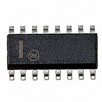
MC26LS30DR2G ON Semiconductor, MC26LS30DR2G Datasheet - Page 2

MC26LS30DR2G
Manufacturer Part Number
MC26LS30DR2G
Description
IC DRIVER LINE CONFIG 16SOIC
Manufacturer
ON Semiconductor
Type
Driverr
Datasheet
1.MC26LS30DG.pdf
(14 pages)
Specifications of MC26LS30DR2G
Number Of Drivers/receivers
4/0
Protocol
RS422, RS423
Voltage - Supply
4.75 V ~ 5.25 V
Mounting Type
Surface Mount
Package / Case
16-SOIC (3.9mm Width)
Lead Free Status / RoHS Status
Lead free / RoHS Compliant
Other names
MC26LS30DR2GOS
MC26LS30DR2GOS
MC26LS30DR2GOSTR
MC26LS30DR2GOS
MC26LS30DR2GOSTR
Maximum ratings are those values beyond which device damage can occur. Maximum ratings applied to the device are individual stress limit
values (not normal operating conditions) and are not valid simultaneously. If these limits are exceeded, device functional operation is not implied,
damage may occur and reliability may be affected.
Devices should not be operated at these limits. The “Recommended Operating Conditions” table provides conditions for actual device operation.
MAXIMUM OPERATING CONDITIONS
RECOMMENDED OPERATING CONDITIONS
All limits are not necessarily functional concurrently.
Power Supply Voltage
Input Voltage (All Inputs)
Applied Output Voltage when in High Impedance Mode
Output Voltage with V
Output Current
Junction Temperature
Power Supply Voltage (Differential Mode)
Power Supply Voltage (Single−Ended Mode)
Input Voltage (All Inputs)
Applied Output Voltage (when in High Impedance Mode)
Applied Output Voltage, V
Output Current
Operating Ambient Temperature (See text)
(V
CC
= 5.0 V, Pin 4 = Logic 0, Pins 3, 6 = Logic 1)
CC
, V
CC
EE
= 0
= 0 V
Rating
Rating
(Pin numbers refer to SO−16 package only.)
http://onsemi.com
MC26LS30
2
Symbol
V
V
V
V
V
V
V
T
I
CC
EE
CC
EE
O
za
zb
in
A
Symbol
V
V
V
V
V
+4.75
+4.75
−5.25
I
T
−0.5
CC
EE
O
Min
−10
−10
−65
−40
za
zb
in
J
0
+5.0
−5.0
Typ
5.0
0
−
−
−
−
−
Self limiting
−0.5, +7.0
−7.0, +0.5
−65, +150
−0.5, +20
Value
15
15
+5.25
+5.25
−4.75
Max
+0.3
+15
+10
+10
+65
+85
Unit
Vdc
Vdc
Unit
Vdc
Vdc
Vdc
mA
−
C
C


