A000003 Arduino, A000003 Datasheet - Page 134
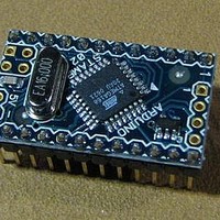
A000003
Manufacturer Part Number
A000003
Description
MCU, MPU & DSP Development Tools MINI
Manufacturer
Arduino
Series
-r
Type
MCUr
Specifications of A000003
Processor To Be Evaluated
Atmega328
Processor Series
ATmega
Data Bus Width
8 bit
Interface Type
USB, RS-232
Operating Supply Voltage
7 V to 9 V
Contents
Board
Lead Free Status / Rohs Status
Lead free / RoHS Compliant
For Use With/related Products
ATmega168


15.11.7
15.11.8
134
ATmega48/88/168
ICR1H and ICR1L – Input Capture Register 1
TIMSK1 – Timer/Counter1 Interrupt Mask Register
The Input Capture is updated with the counter (TCNT1) value each time an event occurs on the
ICP1 pin (or optionally on the Analog Comparator output for Timer/Counter1). The Input Capture
can be used for defining the counter TOP value.
The Input Capture Register is 16-bit in size. To ensure that both the high and low bytes are read
simultaneously when the CPU accesses these registers, the access is performed using an 8-bit
temporary High Byte Register (TEMP). This temporary register is shared by all the other 16-bit
registers.
• Bit 7, 6 – Res: Reserved Bits
These bits are unused bits in the ATmega48/88/168, and will always read as zero.
• Bit 5 – ICIE1: Timer/Counter1, Input Capture Interrupt Enable
When this bit is written to one, and the I-flag in the Status Register is set (interrupts globally
enabled), the Timer/Counter1 Input Capture interrupt is enabled. The corresponding Interrupt
Vector (see “Interrupts” on page 55) is executed when the ICF1 Flag, located in TIFR1, is set.
• Bit 4, 3 – Res: Reserved Bits
These bits are unused bits in the ATmega48/88/168, and will always read as zero.
• Bit 2 – OCIE1B: Timer/Counter1, Output Compare B Match Interrupt Enable
When this bit is written to one, and the I-flag in the Status Register is set (interrupts globally
enabled), the Timer/Counter1 Output Compare B Match interrupt is enabled. The corresponding
Interrupt Vector (see “Interrupts” on page 55) is executed when the OCF1B Flag, located in
TIFR1, is set.
• Bit 1 – OCIE1A: Timer/Counter1, Output Compare A Match Interrupt Enable
When this bit is written to one, and the I-flag in the Status Register is set (interrupts globally
enabled), the Timer/Counter1 Output Compare A Match interrupt is enabled. The corresponding
Interrupt Vector (see “Interrupts” on page 55) is executed when the OCF1A Flag, located in
TIFR1, is set.
• Bit 0 – TOIE1: Timer/Counter1, Overflow Interrupt Enable
When this bit is written to one, and the I-flag in the Status Register is set (interrupts globally
enabled), the Timer/Counter1 Overflow interrupt is enabled. The corresponding Interrupt Vector
(See
Bit
(0x87)
(0x86)
Read/Write
Initial Value
Bit
(0x6F)
Read/Write
Initial Value
“Interrupts” on page
See “Accessing 16-bit Registers” on page 109.
R/W
R
7
0
7
–
0
R/W
55) is executed when the TOV1 Flag, located in TIFR1, is set.
R
6
–
0
6
0
ICIE1
R/W
R/W
5
0
5
0
R/W
R
4
–
0
4
0
ICR1[15:8]
ICR1[7:0]
R/W
R
3
–
0
3
0
OCIE1B
R/W
R/W
2
0
2
0
OCIE1A
R/W
R/W
1
0
1
0
TOIE1
R/W
R/W
0
0
0
0
2545S–AVR–07/10
TIMSK1
ICR1H
ICR1L
Related parts for A000003
Image
Part Number
Description
Manufacturer
Datasheet
Request
R

Part Number:
Description:
Daughter Cards & OEM Boards ARDUINO UNO PROTO PCB REV 3
Manufacturer:
Arduino
Part Number:
Description:
Daughter Cards & OEM Boards ARDUINO SHIELD PROTO KIT REV 3
Manufacturer:
Arduino
Part Number:
Description:
Daughter Cards & OEM Boards ARDUINO MEGA PROTO KIT REV 3
Manufacturer:
Arduino
Part Number:
Description:
Daughter Cards & OEM Boards ARDUINO MEGA PROTO PCB REV 3
Manufacturer:
Arduino
Part Number:
Description:
Development Boards & Kits - AVR ARDUINO STARTER KIT W/ UNO REV3
Manufacturer:
Arduino
Part Number:
Description:
RF Development Tools ARDUINO SHIELD WIRELESS PROTO
Manufacturer:
Arduino
Datasheet:
Part Number:
Description:
RF Development Tools ARDUINO SHIELD WIRELESS WITH SD
Manufacturer:
Arduino
Datasheet:

Part Number:
Description:
Development Software Getting started w/Arduino
Manufacturer:
Arduino

Part Number:
Description:
Ethernet Modules & Development Tools Ethernet Shield for Arduino
Manufacturer:
Arduino

Part Number:
Description:
MCU, MPU & DSP Development Tools LilyPad Arduino Main Board
Manufacturer:
Arduino

Part Number:
Description:
ARDUINO NANO Board
Manufacturer:
Arduino
Datasheet:
Part Number:
Description:
Ethernet Modules & Development Tools ETHERNET SHEILD PoE FOR ARDUINO
Manufacturer:
Arduino
Datasheet:

Part Number:
Description:
ATMEGA328 MCU IC W/ Arduino UNO Bootloader
Manufacturer:
Arduino
Datasheet:
Part Number:
Description:
Memory Cards MICRO SD CARD 1GB WITH SD ADAPTER
Manufacturer:
Arduino