CY7C4292-15ASC Cypress Semiconductor Corp, CY7C4292-15ASC Datasheet
CY7C4292-15ASC
Specifications of CY7C4292-15ASC
Available stocks


Related parts for CY7C4292-15ASC


CY7C4292-15ASC Summary of contents
Page 1
... Functional Description The CY7C4282/CY7C4292 are high-speed, low-power, FIFO memories with clocked read and write interfaces. All devices are nine bits wide. The CY7C4282/CY7C4292 can be cascaded to increase FIFO depth. Programmable features include Almost Full/Almost Empty flags. These FIFOs provide solutions for a wide variety of data buffering needs, including high-speed data acquisition, multiprocessor interfaces, video and communications buffering ...
Page 2
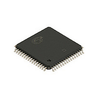
... LD is asserted, WCLK writes data into the programmable flag-offset register. Document #: 38-06009 Rev. *B STQFP Top View CY7C4282 CY7C4292 7C4282/92-10 7C4282/92-15 100 0 CY7C4282 128k x 9 64-pin 10x10 STQFP Description CY7C4282 CY7C4292 GND GND N GND FL/RT N/C 7C4282/92-25 Unit 66.7 40 MHz CY7C4292 Page [+] Feedback ...
Page 3
... FIFO is full, and underflow circuitry to disallow additional reads when the FIFO is empty. An empty FIFO ) go LOW 0 8 maintains the data of the last valid read on its Q even after additional reads occur. after RS is taken RSF CY7C4282 CY7C4292 ; all SS ENS 0–8 outputs 0–8 outputs 0–8 ...
Page 4
... LOW-to-HIGH transition of WCLK by one flip-flop and is set LOW when the number of unread words in the FIFO 0 is greater than or equal to CY7C4282 (64K – m) and CY7C4292 (128K – m). PAF is set HIGH by the LOW-to-HIGH (MSB) Default Value = 000h transition of WCLK when the number of available memory locations is greater than m ...
Page 5
... Programmable Almost Empty/Almost Full Flag The CY7C4282/CY7C4292 features programmable Almost Empty and Almost Full Flags. Each flag can be programmed (described in the Programming section) a specific distance from the corresponding boundary flags (Empty or Full). When the FIFO contains the number of words or fewer for which the ...
Page 6
... Figure 2. Block Diagram of 64K × 9/128K × Deep Sync FIFO Memory Used Document #: 38-06009 Rev. *B RESET (RS) 9 CY7C4282/ FIRST LOAD (FL) EXPANSION IN (XI Width Expansion Configuration CY7C4282 CY7C4292 READ CLOCK (RCLK) READ ENABLE (REN) OUTPUT ENABLE (OE) PROGRAMMABLE (PAF) EMPTY FLAG (EF) EF DATA OUT ( Page [+] Feedback ...
Page 7
... Programmable Flags used in Depth Expansion Configuration Document #: 38-06009 Rev RCLK WCLK REN WEN OE RS 7C4282 D 7C4292 RCLK WCLK REN WEN OE RS 7C4282 D 7C4292 READ CLOCK (RCLK) XO WCLK RCLK READ ENABLE (REN) WEN REN OUTPUTENABLE (OE) RS 7C4282 OE 7C4292 CY7C4282 CY7C4292 DATA OUT (Q) EF Page [+] Feedback ...
Page 8
... CC Com’l 40 Ind 45 Com’l 2 Ind 2 Test Conditions MHz 5.0V CC [10, 11] 3.0V R2 GND 680 3 ns 1.91V CY7C4282 CY7C4292 0. +0.5V CC Ambient Temperature V CC 0°C to +70°C 5V 10% 40°C to +85°C 5V 10% Min. Max. Min. Max. Unit 2.4 2.4 V 0.4 0.4 V 2.0 V 2.0 ...
Page 9
... Almost-Empty Flag and Almost-Full Flag Notes: 12. Pulse widths less than minimum values are not allowed. 13. Values guaranteed by design, not currently tested. Document #: 38-06009 Rev. *B 7C4282/92-10 7C4282/92-15 Min. Max. Min. 100 4 [13 [13 CY7C4282 CY7C4292 7C4282/92-25 Max. Min. Max. Unit 66.7 40 MHz ...
Page 10
... CLK t CLKL NO OPERATION t REF VALID DATA t OE [15] t SKEW1 , then FF may not change state until the next WCLK rising edge. SKEW1 , then EF may not change state until the next RCLK rising edge. SKEW2 CY7C4282 CY7C4292 NO OPERATION t WFF REF t OHZ Page [+] Feedback ...
Page 11
... The first word is available the cycle after EF goes HIGH, always. Document #: 38-06009 Rev RSS RSR t RSF t RSF t RSF [19] t FRL t REF OLZ When t < minimum specification, t CLK SKEW2 SKEW1 CY7C4282 CY7C4292 [18] OE=1 OE [20 4282–9 (maximum) = either 2 FRL CLK SKEW1 CLK SKEW1 Page [+] Feedback ...
Page 12
... DATA IN OUTPUT REGISTER Q – Document #: 38-06009 Rev DATA WRITE 2 t ENS REF REF SKEW1 t A [14 SKEW1 DATA WRITE t WFF t ENS DATA READ CY7C4282 CY7C4292 t ENH [19] t FRL t REF DATA READ NO WRITE DATA WRITE t WFF t ENH t A NEXT DATA READ Page [+] Feedback ...
Page 13
... ENS ENH Note [22] t PAE t ENS 24 Note t CLKL t t ENS ENH t PAF t t ENS (m 1) words of the FIFO when PAF goes LOW. CY7C4282 CY7C4292 WORDS 23 Note IN FIFO t PAE t t ENS ENH FULL M WORDS [25] IN FIFO [26] t PAF SKEW2 t t ENS ENH ...
Page 14
... Document #: 38-06009 Rev CLKL t ENH t DH PAE OFFSET PAF OFFSET LSB MSB t CLKL t ENH t A UNKNOWN PAE OFFSET LSB t PRT to update these flags. RTR CY7C4282 CY7C4292 PAF OFFSET LSB MSB PAF OFFSET MSB PAF OFFSET PAE OFFSET MSB LSB t RTR . RTR Page [+] Feedback ...
Page 15
... Speed (ns) Ordering Code 10 CY7C4292-10ASC CY7C4292-10ASI 15 CY7C4292-15ASC 25 CY7C4292-25ASC Package Diagram 64-Pin Thin Plastic Quad Flat Pack ( 1.4 mm) A64 All product and company names mentioned in this document are the trademarks of their respective holders. Document #: 38-06009 Rev. *B © Cypress Semiconductor Corporation, 2003. The information contained herein is subject to change without notice. Cypress Semiconductor Corporation assumes no responsibility for the use of any circuitry other than circuitry embodied in a Cypress Semiconductor product ...
Page 16
... Document History Page Document Title: CY7C4282/CY7C4292 64K/128K × 9 Deep Sync FIFOs with Retransmit and Depth Expansion Document Number: 38-06009 REV. ECN NO. Issue Date ** 106470 07/17/01 *A 122261 12/26/02 *B 127855 08/25/03 Document #: 38-06009 Rev. *B Orig. of Change Description of Change SZV Changed from Spec Number: 38-00594 to 38-06009 ...