Si5327-EVB Silicon Laboratories Inc, Si5327-EVB Datasheet - Page 49
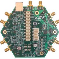
Si5327-EVB
Manufacturer Part Number
Si5327-EVB
Description
MCU, MPU & DSP Development Tools SI5327 EVAL BOARD
Manufacturer
Silicon Laboratories Inc
Specifications of Si5327-EVB
Processor To Be Evaluated
Si5327
Interface Type
I2C, SPI
Operating Supply Voltage
3.3 V
Lead Free Status / Rohs Status
Details


7. Pin Descriptions: Si5327
19, 20, 30,
Note: Internal register names are indicated by underlined italics, e.g., INT_PIN. See Section “5.Register Map”.
2, 9, 14,
Pin #
33
1
3
INT_LOS1
Pin Name
RST
NC
I/O
O
I
INT_LOS1
Signal Level
LOS2
LVCMOS
LVCMOS
GND
VDD
RST
NC
XB
NC
XA
1
2
3
4
5
6
7
8
9
36
10 11 12 13 14 15 16 17
35
External Reset.
Active low input that performs external hardware reset of device.
Resets all internal logic to a known state and forces the device reg-
isters to their default value. Clock outputs are tristated during reset.
The part must be programmed after a reset or power on to get a
clock output. See the Si53xx Family Reference Manual for details.
This pin has a weak pull-up.
No Connection.
Leave floating. Make no external connections to this pin for normal
operation.
Interrupt/CKIN1 LOS Indicator.
This pin functions as a device interrupt output or an alarm output for
CKIN1. If used as an interrupt output, INT_PIN must be set to 1. The
pin functions as a maskable interrupt output with active polarity con-
trolled by the INT_POL register bit.
If used as an alarm output, the pin functions as a LOS alarm indica-
tor for CKIN1. Set CK1_BAD_PIN = 1 and INT_PIN = 0.
0 = CKIN1 present
1 = LOS on CKIN1
The active polarity is controlled by CK_BAD_POL. If no function is
selected, the pin tristates.
Preliminary Rev. 0.4
34
33
GND
Pad
32
31
30
29
28
18
27
26
25
24
23
22
21
20
19
Description
SDI
A2_SS
A1
A0
SDA_SDO
SCL
CKSEL
NC
NC
Si5327
49
Related parts for Si5327-EVB
Image
Part Number
Description
Manufacturer
Datasheet
Request
R

Part Number:
Description:
SMD/C°/SINGLE-ENDED OUTPUT SILICON OSCILLATOR
Manufacturer:
Silicon Laboratories Inc
Part Number:
Description:
Manufacturer:
Silicon Laboratories Inc
Datasheet:
Part Number:
Description:
N/A N/A/SI4010 AES KEYFOB DEMO WITH LCD RX
Manufacturer:
Silicon Laboratories Inc
Datasheet:
Part Number:
Description:
N/A N/A/SI4010 SIMPLIFIED KEY FOB DEMO WITH LED RX
Manufacturer:
Silicon Laboratories Inc
Datasheet:
Part Number:
Description:
N/A/-40 TO 85 OC/EZLINK MODULE; F930/4432 HIGH BAND (REV E/B1)
Manufacturer:
Silicon Laboratories Inc
Part Number:
Description:
EZLink Module; F930/4432 Low Band (rev e/B1)
Manufacturer:
Silicon Laboratories Inc
Part Number:
Description:
I°/4460 10 DBM RADIO TEST CARD 434 MHZ
Manufacturer:
Silicon Laboratories Inc
Part Number:
Description:
I°/4461 14 DBM RADIO TEST CARD 868 MHZ
Manufacturer:
Silicon Laboratories Inc
Part Number:
Description:
I°/4463 20 DBM RFSWITCH RADIO TEST CARD 460 MHZ
Manufacturer:
Silicon Laboratories Inc
Part Number:
Description:
I°/4463 20 DBM RADIO TEST CARD 868 MHZ
Manufacturer:
Silicon Laboratories Inc
Part Number:
Description:
I°/4463 27 DBM RADIO TEST CARD 868 MHZ
Manufacturer:
Silicon Laboratories Inc
Part Number:
Description:
I°/4463 SKYWORKS 30 DBM RADIO TEST CARD 915 MHZ
Manufacturer:
Silicon Laboratories Inc
Part Number:
Description:
N/A N/A/-40 TO 85 OC/4463 RFMD 30 DBM RADIO TEST CARD 915 MHZ
Manufacturer:
Silicon Laboratories Inc
Part Number:
Description:
I°/4463 20 DBM RADIO TEST CARD 169 MHZ
Manufacturer:
Silicon Laboratories Inc