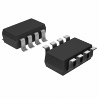
MAX9171EKA+T Maxim Integrated Products, MAX9171EKA+T Datasheet - Page 3

MAX9171EKA+T
Manufacturer Part Number
MAX9171EKA+T
Description
IC RECEIVER LVDS LINE SOT23-8
Manufacturer
Maxim Integrated Products
Type
Receiverr
Datasheet
1.MAX9171EKAT.pdf
(12 pages)
Specifications of MAX9171EKA+T
Number Of Drivers/receivers
0/1
Protocol
LVDS
Voltage - Supply
3 V ~ 3.6 V
Mounting Type
Surface Mount
Package / Case
SOT-23-8
Lead Free Status / RoHS Status
Lead free / RoHS Compliant
SWITCHING CHARACTERISTICS
(V
3.3V, T
Note 1: Current into a pin is defined as positive. Current out of a pin is defined as negative. All voltages are referenced to GND
Note 2: All devices are 100% production tested at T
Note 3: Short only one output at a time. Do not exceed the absolute maximum junction temperature specification.
Note 4: AC parameters are guaranteed by design and not production tested.
Note 5: C
Note 6: Pulse generator output conditions: t
Note 7: t
Note 8: t
Note 9: t
Note 10: t
Differential Propagation Delay
High to Low
Differential Propagation Delay
Low to High
Differential Pulse Skew
|t
Differential Channel-to-Channel
Skew (MAX9172)
Differential Part-to-Part Skew
Rise Time
Fall Time
Maximum Operating Frequency
PHLD
CC
= 3.0V to 3.6V, C
A
- t
= +25°C.) (Notes 4, 5, 6)
except V
the same part.
5°C of each other.
supply and temperature ranges.
PLHD
SKD1
SKD2
SKD3
SKD4
PARAMETER
L
includes scope probe and test jig capacitance.
|
is the magnitude of the difference of differential propagation delays in a channel. t
is the magnitude of the difference of the t
is the magnitude of the difference of any differential propagation delays between parts at the same V
is the magnitude of the difference of any differential propagation delays between parts operating over the rated
TH
, V
_______________________________________________________________________________________
L
TL
= 15pF, |V
, and V
Single/Dual LVDS Line Receivers with
ID
.
ID
| = 0.2V, V
SYMBOL
t
t
t
t
t
t
f
PHLD
PLHD
SKD1
SKD2
SKD3
SKD4
t
t
MAX
TLH
THL
R
= t
CM
F
< 1ns (0% to 100%), frequency = 250MHz, 50% duty cycle, V
Figures 2, 3
Figures 2, 3
Figures 2, 3 (Note 7)
Figures 2, 3 (Note 8)
Figures 2, 3 (Note 9)
Figures 2, 3 (Note 10)
Figures 2, 3
Figures 2, 3
All channels switching, V
V
= 1.2V, T
OH(MIN)
A
= +25°C and are guaranteed by design for T
PLHD
= 2.7V, 40% < duty cycle < 60%
A
= -40°C to +85°C, unless otherwise noted. Typical values are at V
or t
CONDITIONS
PHLD
of one channel and the t
OL(MAX)
“In-Path” Fail-Safe
= 0.4V,
PLHD
SKD1
MIN
A
250
1.0
1.0
= -40°C to +85°C, as specified.
or t
= |t
PHLD
PHLD
TYP
1.65
1.62
0.55
0.51
300
30
40
OH
of the other channel on
- t
= 1.3V, V
PLHD
MAX
CC
400
500
2.5
2.5
1.5
0.8
0.8
1
|.
and within
OL
= 1.1V.
UNITS
MHz
ps
ps
ns
ns
ns
ns
ns
CC
3
=


