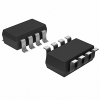
MAX9171EKA+T Maxim Integrated Products, MAX9171EKA+T Datasheet - Page 7

MAX9171EKA+T
Manufacturer Part Number
MAX9171EKA+T
Description
IC RECEIVER LVDS LINE SOT23-8
Manufacturer
Maxim Integrated Products
Type
Receiverr
Datasheet
1.MAX9171EKAT.pdf
(12 pages)
Specifications of MAX9171EKA+T
Number Of Drivers/receivers
0/1
Protocol
LVDS
Voltage - Supply
3 V ~ 3.6 V
Mounting Type
Surface Mount
Package / Case
SOT-23-8
Lead Free Status / RoHS Status
Lead free / RoHS Compliant
Figure 1. Input with In-Path Fail-Safe Network Equivalent Circuit
Figure 2. Propagation Delay and Transition Test Time Circuit
Figure 3. Propagation Delay and Transition Time Waveforms
GENERATOR
PULSE
IN_-
IN_+
OUT_
IN_+
IN_-
V
_______________________________________________________________________________________
CC
50Ω
2.5µA
5µA
Single/Dual LVDS Line Receivers with
40mV
1.2V (0V DIFFERENTIAL)
t
PLHD
20%
50Ω
IN_+
IN_-
t
TLH
1.5V
80%
OUT_
OUT_
15pF
The MAX9171/MAX9172 have in-path fail-safe that is
compatible with in-path fail-safe receivers, such as the
DS90LV018A and DS90LV028A. Refer to the MAX9111/
MAX9113 data sheet for pin-compatible receivers with
parallel fail-safe and lower jitter. Refer to the MAX9130
data sheet for a single LVDS receiver with parallel fail-
safe in an SC70 package.
The MAX9171/MAX9172 with in-path fail-safe are
designed with a +40mV input offset voltage, a 2.5µA
current source between V
input, and a 5µA current sink between the inverting
input and ground (Figure 1). If the differential input is
open, the 2.5µA current source pulls the input to V
0.7V and the 5µA source sink pulls the inverting input to
ground, which drives the receiver output high. If the dif-
ferential input is shorted or terminated with a typical
value termination resistor, the +40mV offset drives the
receiver output high. If the input is terminated and float-
ing, the receiver output is driven high by the +40mV off-
set, and the 2:1 current sink to current source ratio
(5µA:2.5µA) pulls the inputs to ground. This can be an
advantage when switching between drivers on a multi-
point bus because the change in common-mode volt-
age from ground to the typical driver offset voltage of
1.2V is not as much as the change from V
(parallel fail-safe pulls the bus to V
the propagation delay and transition test time circuit
and Figure 3 shows the propagation delay and transi-
tion test time waveforms.
“In-Path” Fail-Safe
In-Path vs. Parallel Fail-Safe
t
PHLD
80%
1.5V
CC
V
ID
t
THL
and the noninverting
= 0.2V
CC
20%
). Figure 2 shows
1.3V
1.1V
V
V
OH
OL
CC
to 1.2V
CC
7
-


