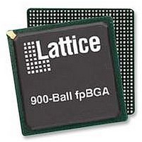
LFE2M70E-5FN900C Lattice, LFE2M70E-5FN900C Datasheet - Page 103

LFE2M70E-5FN900C
Manufacturer Part Number
LFE2M70E-5FN900C
Description
IC, LATTICEECP2M FPGA, 420MHZ, FPBGA-900
Manufacturer
Lattice
Series
LatticeECP2Mr
Datasheet
1.LFE2-12E-5FN256C.pdf
(385 pages)
Specifications of LFE2M70E-5FN900C
No. Of Logic Blocks
67000
No. Of Macrocells
34000
No. Of Speed Grades
5
Total Ram Bits
4534Kbit
No. Of I/o's
416
Clock Management
DLL, PLL
I/o Supply Voltage
3.465V
Rohs Compliant
Yes
Lead Free Status / Rohs Status
Lead free / RoHS Compliant
Available stocks
Company
Part Number
Manufacturer
Quantity
Price
Company:
Part Number:
LFE2M70E-5FN900C
Manufacturer:
Lattice Semiconductor Corporation
Quantity:
10 000
- Current page: 103 of 385
- Download datasheet (3Mb)
Signal Descriptions (Cont.)
Lattice Semiconductor
[LOC]_SQ_VCCOBm
[LOC]_SQ_HDOUTNm
[LOC]_SQ_HDOUTPm
[LOC]_SQ_HDINNm
[LOC]_SQ_HDINPm
[LOC]_SQ_VCCTXm
[LOC]_SQ_VCCRXm
1. These signals are relevant for LatticeECP2M family.
2. m defines the associated channel in the Quad.
3. These signals are defined in Quads [LOC] indicates the corner SERDES Quad is located: ULC (upper left), URC (upper right), LLC (lower
4. When placing switching I/Os around these critical pins that are designed to supply the device with the proper reference or supply voltage,
left), LRC (lower right).
care must be given. For more information, refer to technical note TN1159, LatticeECP2/M Pin Assignment Recommendations.
Signal Name
4
4
I/O
—
—
—
O
O
I
I
Output buffer power supply, channel m (1.2V/1.5V). This pin should be left
floating if the channel is unused.
High-speed output, negative channel m
High-speed output, positive channel m
High-speed input, negative channel m
High-speed input, positive channel m
Transmitter power supply, channel m (1.2V). This pin must be tied to 1.2V
even if the channel is unused.
Receiver power supply, channel m (1.2V). This pin must be tied to 1.2V even if
the channel is unused.
4-3
LatticeECP2/M Family Data Sheet
Description
Pinout Information
Related parts for LFE2M70E-5FN900C
Image
Part Number
Description
Manufacturer
Datasheet
Request
R
Part Number:
Description:
Manufacturer:
Lattice Semiconductor Corp.
Datasheet:
Part Number:
Description:
IC, LATTICEECP2M FPGA, 420MHZ, FPBGA-900
Manufacturer:
LATTICE SEMICONDUCTOR
Datasheet:

Part Number:
Description:
IC FPGA 50KLUTS 410I/O 900-BGA
Manufacturer:
Lattice
Datasheet:

Part Number:
Description:
IC FPGA 50KLUTS 410I/O 900-BGA
Manufacturer:
Lattice
Datasheet:

Part Number:
Description:
IC FPGA 67KLUTS 1152FPBGA
Manufacturer:
Lattice
Datasheet:

Part Number:
Description:
IC FPGA 67KLUTS 900FPBGA
Manufacturer:
Lattice
Datasheet:

Part Number:
Description:
IC FPGA 67KLUTS 1152FPBGA
Manufacturer:
Lattice
Datasheet:

Part Number:
Description:
IC FPGA 67KLUTS 1152FPBGA
Manufacturer:
Lattice
Datasheet:

Part Number:
Description:
IC FPGA 67KLUTS 1152FPBGA
Manufacturer:
Lattice
Datasheet:

Part Number:
Description:
FPGA - Field Programmable Gate Array 67K LUTs 430 I/O Memry DSP 1.2V -5Spd
Manufacturer:
Lattice

Part Number:
Description:
FPGA - Field Programmable Gate Array 67K LUTs 430 I/O Memry DSP 1.2V -7Spd
Manufacturer:
Lattice

Part Number:
Description:
FPGA - Field Programmable Gate Array 67K LUTs 430 I/O Memry DSP 1.2V -5Spd
Manufacturer:
Lattice

Part Number:
Description:
FPGA - Field Programmable Gate Array 67K LUTs 430 I/O Memry DSP 1.2V -6Spd
Manufacturer:
Lattice

Part Number:
Description:
FPGA - Field Programmable Gate Array 67K LUTs 416 I/O Memory DSP 1.2V 5SPD
Manufacturer:
Lattice


