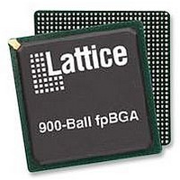
LFE2M70E-5FN900C Lattice, LFE2M70E-5FN900C Datasheet - Page 5

LFE2M70E-5FN900C
Manufacturer Part Number
LFE2M70E-5FN900C
Description
IC, LATTICEECP2M FPGA, 420MHZ, FPBGA-900
Manufacturer
Lattice
Series
LatticeECP2Mr
Datasheet
1.LFE2-12E-5FN256C.pdf
(385 pages)
Specifications of LFE2M70E-5FN900C
No. Of Logic Blocks
67000
No. Of Macrocells
34000
No. Of Speed Grades
5
Total Ram Bits
4534Kbit
No. Of I/o's
416
Clock Management
DLL, PLL
I/o Supply Voltage
3.465V
Rohs Compliant
Yes
Lead Free Status / Rohs Status
Lead free / RoHS Compliant
Available stocks
Company
Part Number
Manufacturer
Quantity
Price
Company:
Part Number:
LFE2M70E-5FN900C
Manufacturer:
Lattice Semiconductor Corporation
Quantity:
10 000
- Current page: 5 of 385
- Download datasheet (3Mb)
Lattice Semiconductor
Figure 2-1. Simplified Block Diagram, ECP2-6 Device (Top Level)
sysCLOCK PLLs and DLLs
Frequency Synthesis and
Clock Alignment
Figure 2-2. Simplified Block Diagram, ECP2M20 Device (Top Level)
Configuration
Logic, Including
dual boot and encryption,
and soft-error detection
Programmable
Function Units
(PFUs)
sysDSP Blocks
Multiply and
Accumulate Support
sysMEM Block RAM
18kbit Dual Port
Flexible sysIO
Buffers:
LVCMOS, HSTL
SSTL, LVDS
Programmable
Function Units
(PFUs)
DSP Blocks
Multiply & Accumulate
Support
sysMEM Block
RAM 18kbit Dual Port
On-Chip
Oscillator
2-2
Channel
3
Channel
2
LatticeECP2/M Family Data Sheet
Channel
1
Channel
0
Flexible sysIO Buffers:
LVCMOS, HSTL, SSTL,
LVDS, and other standards
Pre-engineered source
synchronous support
• DDR1/2
• SPI4.2
• ADC/DAC devices
Flexible routing optimized
for speed, cost and routability
Configuration logic, including
dual boot and encryption.
On-chip oscillator and
soft-error detection.
Configuration port
SERDES
Pre-Engineered
Source Synchronous
Support
• DDR1/2
• SPI4.2
• ADC/DAC devices
sysCLOCK SPLLs
Flexible Routing
optimized for speed,
cost & routability
sysCLOCK GPLLs
& GDLLs
Frequency Synthesis
& Clock Alignment
Configuration Port
Architecture
Related parts for LFE2M70E-5FN900C
Image
Part Number
Description
Manufacturer
Datasheet
Request
R
Part Number:
Description:
Manufacturer:
Lattice Semiconductor Corp.
Datasheet:
Part Number:
Description:
IC, LATTICEECP2M FPGA, 420MHZ, FPBGA-900
Manufacturer:
LATTICE SEMICONDUCTOR
Datasheet:

Part Number:
Description:
IC FPGA 50KLUTS 410I/O 900-BGA
Manufacturer:
Lattice
Datasheet:

Part Number:
Description:
IC FPGA 50KLUTS 410I/O 900-BGA
Manufacturer:
Lattice
Datasheet:

Part Number:
Description:
IC FPGA 67KLUTS 1152FPBGA
Manufacturer:
Lattice
Datasheet:

Part Number:
Description:
IC FPGA 67KLUTS 900FPBGA
Manufacturer:
Lattice
Datasheet:

Part Number:
Description:
IC FPGA 67KLUTS 1152FPBGA
Manufacturer:
Lattice
Datasheet:

Part Number:
Description:
IC FPGA 67KLUTS 1152FPBGA
Manufacturer:
Lattice
Datasheet:

Part Number:
Description:
IC FPGA 67KLUTS 1152FPBGA
Manufacturer:
Lattice
Datasheet:

Part Number:
Description:
FPGA - Field Programmable Gate Array 67K LUTs 430 I/O Memry DSP 1.2V -5Spd
Manufacturer:
Lattice

Part Number:
Description:
FPGA - Field Programmable Gate Array 67K LUTs 430 I/O Memry DSP 1.2V -7Spd
Manufacturer:
Lattice

Part Number:
Description:
FPGA - Field Programmable Gate Array 67K LUTs 430 I/O Memry DSP 1.2V -5Spd
Manufacturer:
Lattice

Part Number:
Description:
FPGA - Field Programmable Gate Array 67K LUTs 430 I/O Memry DSP 1.2V -6Spd
Manufacturer:
Lattice

Part Number:
Description:
FPGA - Field Programmable Gate Array 67K LUTs 416 I/O Memory DSP 1.2V 5SPD
Manufacturer:
Lattice


