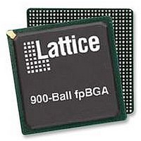
LFE2M70E-5FN900C Lattice, LFE2M70E-5FN900C Datasheet - Page 19

LFE2M70E-5FN900C
Manufacturer Part Number
LFE2M70E-5FN900C
Description
IC, LATTICEECP2M FPGA, 420MHZ, FPBGA-900
Manufacturer
Lattice
Series
LatticeECP2Mr
Datasheet
1.LFE2-12E-5FN256C.pdf
(385 pages)
Specifications of LFE2M70E-5FN900C
No. Of Logic Blocks
67000
No. Of Macrocells
34000
No. Of Speed Grades
5
Total Ram Bits
4534Kbit
No. Of I/o's
416
Clock Management
DLL, PLL
I/o Supply Voltage
3.465V
Rohs Compliant
Yes
Lead Free Status / Rohs Status
Lead free / RoHS Compliant
Available stocks
Company
Part Number
Manufacturer
Quantity
Price
Company:
Part Number:
LFE2M70E-5FN900C
Manufacturer:
Lattice Semiconductor Corporation
Quantity:
10 000
- Current page: 19 of 385
- Download datasheet (3Mb)
Lattice Semiconductor
this special vertical routing channel and the eight secondary clock regions for the ECP2-50. LatticeECP2 devices
have eight secondary clock and control signal resources per region (SC0 to SC7).
The secondary clock muxes are located in the center of the device. Figure 2-16 shows the mux structure of the
secondary clock routing.
Figure 2-15. Secondary Clock Regions ECP2-50
Figure 2-16. Secondary Clock Selection
SC0
24:1
Secondary Clock
Secondary Clock
Secondary Clock
Secondary Clock
I/O Bank 0
I/O Bank 5
Region 1
Region 2
Region 3
Region 4
SC1
24:1
Secondary Clock Sources: 8 PIOs + 16 Routing
SC2
24:1
8 Secondary Clocks (SC0 to SC7)
SC3
24:1
Clock/Control
SC4
Secondary Clock
Secondary Clock
Secondary Clock
Secondary Clock
2-16
24:1
I/O Bank 1
I/O Bank 4
Region 5
Region 6
Region 7
Region 8
SC5
24:1
LatticeECP2/M Family Data Sheet
SC6
24:1
SC7
24:1
Vertical Routing
Channel Regional
Boundary
DSP Row
Regional
Boundary
DSP Row
Regional
Boundary
EBR Row
Regional
Boundary
Architecture
Related parts for LFE2M70E-5FN900C
Image
Part Number
Description
Manufacturer
Datasheet
Request
R
Part Number:
Description:
Manufacturer:
Lattice Semiconductor Corp.
Datasheet:
Part Number:
Description:
IC, LATTICEECP2M FPGA, 420MHZ, FPBGA-900
Manufacturer:
LATTICE SEMICONDUCTOR
Datasheet:

Part Number:
Description:
IC FPGA 50KLUTS 410I/O 900-BGA
Manufacturer:
Lattice
Datasheet:

Part Number:
Description:
IC FPGA 50KLUTS 410I/O 900-BGA
Manufacturer:
Lattice
Datasheet:

Part Number:
Description:
IC FPGA 67KLUTS 1152FPBGA
Manufacturer:
Lattice
Datasheet:

Part Number:
Description:
IC FPGA 67KLUTS 900FPBGA
Manufacturer:
Lattice
Datasheet:

Part Number:
Description:
IC FPGA 67KLUTS 1152FPBGA
Manufacturer:
Lattice
Datasheet:

Part Number:
Description:
IC FPGA 67KLUTS 1152FPBGA
Manufacturer:
Lattice
Datasheet:

Part Number:
Description:
IC FPGA 67KLUTS 1152FPBGA
Manufacturer:
Lattice
Datasheet:

Part Number:
Description:
FPGA - Field Programmable Gate Array 67K LUTs 430 I/O Memry DSP 1.2V -5Spd
Manufacturer:
Lattice

Part Number:
Description:
FPGA - Field Programmable Gate Array 67K LUTs 430 I/O Memry DSP 1.2V -7Spd
Manufacturer:
Lattice

Part Number:
Description:
FPGA - Field Programmable Gate Array 67K LUTs 430 I/O Memry DSP 1.2V -5Spd
Manufacturer:
Lattice

Part Number:
Description:
FPGA - Field Programmable Gate Array 67K LUTs 430 I/O Memry DSP 1.2V -6Spd
Manufacturer:
Lattice

Part Number:
Description:
FPGA - Field Programmable Gate Array 67K LUTs 416 I/O Memory DSP 1.2V 5SPD
Manufacturer:
Lattice


