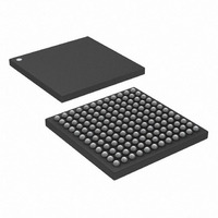
DS3154+ Maxim Integrated Products, DS3154+ Datasheet - Page 30

DS3154+
Manufacturer Part Number
DS3154+
Description
IC LIU DS3/E3/STS1 QUAD 144CSBGA
Manufacturer
Maxim Integrated Products
Type
Line Interface Units (LIUs)r
Datasheet
1.DS3151.pdf
(61 pages)
Specifications of DS3154+
Number Of Drivers/receivers
4/4
Protocol
IEEE 1149.1
Voltage - Supply
3.135 V ~ 3.465 V
Mounting Type
Surface Mount
Package / Case
144-CSBGA
Lead Free Status / RoHS Status
Lead free / RoHS Compliant
the JA must take its master clock from the MCLK pin. The clock and data recovery block also uses the selected
master clock.
The JA has a loop bandwidth of master_clock / 2,058,874 (see corner frequencies in
attenuates jitter at frequencies higher than the loop bandwidth, while allowing jitter (and wander) at lower
frequencies to pass through relatively unaffected.
Figure 9-1. Jitter Attenuation/Jitter Transfer
10.
There are four sources for reset: an internal power-on reset (POR) circuit, the reset pin RST, the JTAG reset pin
JTRST, and the RST bit in each LIU’s global configuration register (GCR). The chip is divided into three zones for
reset: the digital logic, the analog circuits, and the JTAG logic. The digital logic includes the status and control
registers, the B3ZS/HDB3 encoder and decoder, the PRBS generator and detector, and the LOS detect logic. The
analog circuits include clock and data recovery, jitter attenuator, and transmit waveform generation. The JTAG
logic consists of the common boundary scan controller and the boundary scan cells at each pin.
The POR circuit resets the digital logic, analog circuits, and JTAG logic zones. The RST pin resets the digital logic
and the analog circuits but not the JTAG logic. The JTRST pin resets only the JTAG logic. Each LIU’s RST register
bit resets the digital logic for that LIU, including resetting the LIU’s registers to the default state (except for the RST
bit).
The POR signal and RST pin require an active master clock source for the LIU to properly reset.
RESET LOGIC
-10
-20
-30
21.7Hz (DS3)
16.7Hz (E3)
25.2Hz (STS-1)
0
ATTENUATION
ATTENUATOR
DS3/E3/STS-1
WITH JITTER
10
ENABLED
MINIMUM
DS315x
JITTER
27Hz
40Hz
DS3 [GR-253 (1999)]
CATEGORY I
DS3151/DS3152/DS3153/DS3154 Single/Dual/Triple/Quad DS3/E3/STS-1 LIUs
100
1k
1k
FREQUENCY (Hz)
30 of 61
DS3 [GR-499 (1995)]
CATEGORY I
STS-1 [GR-253
CATEGORY II
E3 [TBR24 (1997)]
10k
(1999)]
DS3 [GR-499 (1999)]
40k 59.6k
CATEGORY II
100k
>150k
DS315x TYPICAL RECEIVER
JITTER TRANSFER WITH JITTER
ATTENUATOR DISABLED
1M
Figure
9-1). The JA


