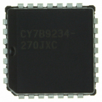
CY7B9234-270JXC Cypress Semiconductor Corp, CY7B9234-270JXC Datasheet - Page 17

CY7B9234-270JXC
Manufacturer Part Number
CY7B9234-270JXC
Description
IC TRANSMITTER HOTLINK 28-PLCC
Manufacturer
Cypress Semiconductor Corp
Series
HOTlink™r
Type
Transmitter and Receiverr
Datasheet
1.CY7B9234-270JXC.pdf
(36 pages)
Specifications of CY7B9234-270JXC
Package / Case
28-PLCC
Protocol
Fibre Channel
Voltage - Supply
4.5 V ~ 5.5 V
Mounting Type
Surface Mount
Product
PHY
Supply Voltage (min)
4.5 V
Supply Current
0.085 A
Maximum Operating Temperature
+ 70 C
Minimum Operating Temperature
0 C
Mounting Style
SMD/SMT
Number Of Channels
1
Lead Free Status / RoHS Status
Lead free / RoHS Compliant
Number Of Drivers/receivers
-
Lead Free Status / RoHS Status
Lead free / RoHS Compliant, Lead free / RoHS Compliant
Other names
428-2905-5
CY7B9234-270JXC
CY7B9234-270JXC
Available stocks
Company
Part Number
Manufacturer
Quantity
Price
Company:
Part Number:
CY7B9234-270JXC
Manufacturer:
CY
Quantity:
10
Company:
Part Number:
CY7B9234-270JXC
Manufacturer:
CYPRESS
Quantity:
831
Company:
Part Number:
CY7B9234-270JXC
Manufacturer:
Cypress Semiconductor Corp
Quantity:
10 000
Company:
Part Number:
CY7B9234-270JXCT
Manufacturer:
Cypress Semiconductor Corp
Quantity:
10 000
Data loaded into the Input register on the rising edge of CKW will
be loaded into the Shifter on the subsequent rising edges of
CKW. It will then be shifted to the outputs one bit at a time using
the internal clock generated by the clock generator. The first bit
of the transmission character (Da) will appear at the output
(OUTA±, OUTB±, and OUTC±) after the next CKW edge.
While in either the Encoded mode or Bypass mode, if a CKW
edge arrives when the inputs are not enabled (ENA and ENN
both HIGH), the Encoder will insert a pad character K28.5 (e.g.,
C5.0) to maintain proper link synchronization (in Bypass mode
the proper sense of running disparity cannot be guaranteed for
the first pad character, but is correct for all pad characters that
follow).
inhibited by insuring that the Transmitter is always enabled (i.e.,
ENA or ENN is hard-wired LOW).
PECL Output Functional and Connection Options
The three pairs of PECL outputs all contain the same information
and are intended for use in systems with multiple connections.
Document #: 38-02014 Rev. *B
This automatic insertion of pad characters can be
ENA
CKR
SMPTE HOTLink TRANSMITTER
ASYNCHRONOUS FIFO
ASYNCHRONOUS FIFO
CKW
SMPTE HOTLink RECEIVER
RDY
7C42X/3X/6X/7X
7C42X/3X/6X/7X
W
7B9234
7B9334
RP
R
Q
Figure 5. Seamless FIFO Interface
D
0 − 7
0 − 7
Q
D
0 − 8
0 − 8
,SC/D
,SC/D
9
9
Each output pair may be connected to a different serial media,
each of which may be a different length, link type, or interface
technology. For systems that do not require all three output
pairs, the unused pairs should be wired to V
power dissipated by the output circuit, and to minimize unwanted
noise generation. An internal voltage comparator detects when
an output differential pair is wired to V
source for that pair to be disabled. This results in a power
savings of around 5 mA for each unused pair.
In systems that require the outputs to be shut off during some
periods when link transmission is prohibited (e.g., for laser safety
functions), the FOTO input can be asserted. While it is possible
to insure that the output state of the PECL drivers is LOW (i.e.,
light is off) by sending all 0’s in Bypass mode, it is often inconve-
nient to insert this level of control into the data transmission
channel, and it is impossible in Encoded mode.
provided to simplify and augment this control function (typically
found in laser-based transmission systems). FOTO will force
OUTA+ and OUTB+ to go LOW, OUTA− and OUTB− to go HIGH,
ENR
ENN
CKR
CKW
SMPTE HOTLink TRANSMITTER
SMPTE HOTLink RECEIVER
CKW
CKR
CLOCKED FIFO
CLOCKED FIFO
RDY
ENW
7C44X/5X
7C44X/5X
7B9234
7B9334
Q
D
0 − 7
0 − 7
Q
D
0 − 8
0 − 8
,SC/D
,SC/D
CC
9
9
, causing the current
CC
CY7B9234
CY7B9334
to minimize the
Page 17 of 36
FOTO is
[+] Feedback


