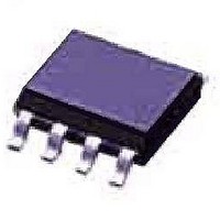
ATTINY12-8SU Atmel, ATTINY12-8SU Datasheet - Page 16

ATTINY12-8SU
Manufacturer Part Number
ATTINY12-8SU
Description
Microcontrollers (MCU) AVR 1K FLASH 64B EE 5V 8MHZ
Manufacturer
Atmel
Datasheet
1.ATTINY12-8SU.pdf
(94 pages)
Specifications of ATTINY12-8SU
Processor Series
ATTINY1x
Core
AVR8
Data Bus Width
8 bit
Program Memory Type
Flash
Program Memory Size
1 KB
Maximum Clock Frequency
8 MHz
Number Of Programmable I/os
6
Number Of Timers
1
Maximum Operating Temperature
+ 85 C
Mounting Style
SMD/SMT
Package / Case
SOIC
3rd Party Development Tools
EWAVR, EWAVR-BL
Development Tools By Supplier
ATAVRDRAGON, ATSTK500
Minimum Operating Temperature
- 40 C
Cpu Family
ATtiny
Device Core
AVR
Device Core Size
8b
Frequency (max)
8MHz
Interface Type
SPI
# I/os (max)
6
Number Of Timers - General Purpose
1
Operating Supply Voltage (typ)
5V
Operating Supply Voltage (max)
5.5V
Operating Supply Voltage (min)
4V
Instruction Set Architecture
RISC
Operating Temp Range
-40C to 85C
Operating Temperature Classification
Industrial
Mounting
Surface Mount
Pin Count
8
Package Type
SOIC EIAJ
Lead Free Status / Rohs Status
Details
Available stocks
Company
Part Number
Manufacturer
Quantity
Price
Company:
Part Number:
ATTINY12-8SU
Manufacturer:
ATMEL
Quantity:
5
Memory Access and
Instruction Execution
Timing
16
ATtiny11/12
Register Operands Fetch
This section describes the general access timing concepts for instruction execution and
internal memory access.
The AVR CPU is driven by the System Clock Ø, directly generated from the external
clock crystal for the chip. No internal clock division is used.
Figure 14 shows the parallel instruction fetches and instruction executions enabled by
the Harvard architecture and the fast-access register file concept. This is the basic pipe-
lining concept to obtain up to 1 MIPS per MHz with the corresponding unique results for
functions per cost, functions per clocks, and functions per power-unit.
Figure 14. The Parallel Instruction Fetches and Instruction Executions
Figure shows the internal timing concept for the register file. In a single clock cycle, an
ALU operation using two register operands is executed and the result is stored back to
the destination register.
Single-cycle ALU Operation
2nd Instruction Execute
3rd Instruction Execute
1st Instruction Execute
ALU Operation Execute
2nd Instruction Fetch
3rd Instruction Fetch
4th Instruction Fetch
1st Instruction Fetch
Total Execution Time
Result Write Back
System Clock Ø
System Clock Ø
T1
T1
T2
T2
T3
T3
1006F–AVR–06/07
T4
T4


