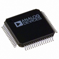
ADV7180BSTZ Analog Devices Inc, ADV7180BSTZ Datasheet - Page 44

ADV7180BSTZ
Manufacturer Part Number
ADV7180BSTZ
Description
IC VIDEO DECODER SDTV 64-LQFP
Manufacturer
Analog Devices Inc
Type
Video Decoderr
Datasheet
1.ADV7180BSTZ.pdf
(116 pages)
Specifications of ADV7180BSTZ
Design Resources
Low Cost Differential Video Receiver Using ADA4851 Amplifier and ADV7180 Video Decoder (CN0060) Low Cost Video Multiplexer for Video Switching Using ADA4853-2 Op Amp with Disable Function (CN0076)
Applications
Digital Cameras, Mobile Phones, Portable Video
Voltage - Supply, Analog
1.71 V ~ 1.89 V
Voltage - Supply, Digital
1.65 V ~ 2 V
Mounting Type
Surface Mount
Package / Case
64-LQFP
Resolution (bits)
10bit
Input Format
Analog
Output Format
Digital
Adc Sample Rate
57.27MSPS
Power Dissipation Pd
15µW
No. Of Input Channels
6
Supply Voltage Range
1.71V To 1.89V
Lead Free Status / RoHS Status
Lead free / RoHS Compliant
For Use With
EVAL-ADV7180LQEBZ - BOARD EVALUATION ADV7180EVAL-ADV7180LFEBZ - BOARD EVAL FOR ADV7180 LFCSP
Lead Free Status / RoHS Status
Lead free / RoHS Compliant, Lead free / RoHS Compliant
Available stocks
Company
Part Number
Manufacturer
Quantity
Price
Company:
Part Number:
ADV7180BSTZ
Manufacturer:
AMIS
Quantity:
6 240
Company:
Part Number:
ADV7180BSTZ
Manufacturer:
Analog Devices Inc
Quantity:
10 000
Part Number:
ADV7180BSTZ
Manufacturer:
ADI/亚德诺
Quantity:
20 000
Company:
Part Number:
ADV7180BSTZ-REEL
Manufacturer:
Analog Devices Inc
Quantity:
10 000
ADV7180
BL_C_VBI, Blank Chroma During VBI, Address 0x04[2]
Setting BL_C_VBI high blanks the Cr and Cb values of all VBI
lines. This is done so any data that may arrive during VBI is not
decoded as color and is output through Cr and Cb. As a result,
it is possible to send VBI lines into the decoder and then output
them through an encoder again, undistorted. Without this
blanking, any color that is incorrectly decoded would be encoded
by the video encoder, thus distorting the VBI lines.
Setting BL_C_VBI to 0 decodes and outputs color during VBI.
Setting BL_C_VBI to 1 (default) blanks Cr and Cb values
during VBI.
Range, Range Selection, Address 0x04[0]
AV codes (as per ITU-R BT.656, formerly known as CCIR-656)
consist of a fixed header made up of 0xFF and 0x00 values.
These two values are reserved and, therefore, are not to be used
for active video. Additionally, the ITU specifies that the nominal
range for video should be restricted to values between 16 and
235 for luma and 16 and 240 for chroma.
The range bit allows the user to limit the range of values output
by the ADV7180 to the recommended value range. In any case,
it ensures that the reserved values of 255d (0xFF) and 00d
(0x00) are not presented on the output pins unless they are part
of an AV code header.
Table 61. RANGE Function
Range
0
1 (default)
AUTO_PDC_EN, Automatic Programmed Delay Control,
Address 0x27[6]
Enabling AUTO_PDC_EN activates a function within the
ADV7180 that automatically programs the LTA[1:0] and CTA[2:0]
registers to have the chroma and luma data match delays for all
modes of operation. If AUTO_PDC__EN is set, the LTA[1:0]
and CTA[2:0] manual registers are not used. If the automatic
mode is disabled (by setting the AUTO_PDC_EN bit to 0), the
values programmed into the LTA[1:0] and CTA[2:0] registers
become active.
When AUTO_PDC_EN is 0, the ADV7180 uses the LTA[1:0] and
CTA[2:0] values for delaying luma and chroma samples. See the
LTA[1:0], Luma Timing Adjust, Address 0x27[1:0] section and
the CTA[2:0], Chroma Timing Adjust, Address 0x27[5:3]
section.
Description
16 ≤ Y ≤ 235, 16 ≤ C/P ≤ 240
1 ≤ Y ≤ 254, 1 ≤ C/P ≤ 254
Rev. F | Page 44 of 116
When AUTO_PDC_EN is 1 (default), the ADV7180 automatically
determines the LTA and CTA values to have luma and chroma
aligned at the output.
LTA[1:0], Luma Timing Adjust, Address 0x27[1:0]
The luma timing adjust register allows the user to specify a
timing difference between chroma and luma samples.
There is a functionality overlap with the CTA[2:0] register. For
manual programming, use the following defaults:
•
•
•
Table 62. LTA Function
LTA[1:0]
00 (default)
01
10
11
CTA[2:0], Chroma Timing Adjust, Address 0x27[5:3]
The chroma timing adjust register allows the user to specify a
timing difference between chroma and luma samples. This can
be used to compensate for external filter group delay differences
in the luma vs. chroma path and to allow a different number of
pipeline delays while processing the video downstream. Review
this functionality together with the LTA[1:0] register.
The chroma can be delayed or advanced only in chroma pixel
steps. One chroma pixel step is equal to two luma pixels. The
programmable delay occurs after demodulation, where delay
cannot be made by luma pixel steps.
For manual programming, use the following defaults:
•
•
•
Table 63. CTA Function
CTA[2:0]
000
001
010
011 (default)
100
101
110
111
CVBS input LTA[1:0] = 00
Y/C input LTA[1:0] = 01
YPrPb input LTA[1:0] = 01
CVBS input CTA[2:0] = 011
Y/C input CTA[2:0] = 101
YPrPb input CTA[2:0] = 110
Description
No delay
Luma 1 clock (37 ns) late
Luma 2 clock (74 ns) early
Luma 1 clock (37 ns) early
Description
Not a valid setting
Chroma + two pixels (early)
Chroma + one pixel (early)
No delay
Chroma − one pixel (late)
Chroma − two pixels (late)
Chroma − three pixels (late)
Not a valid setting


