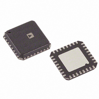
ADV7391BCPZ Analog Devices Inc, ADV7391BCPZ Datasheet - Page 58

ADV7391BCPZ
Manufacturer Part Number
ADV7391BCPZ
Description
IC ENCODER VIDEO W/DAC 32-LFCSP
Manufacturer
Analog Devices Inc
Type
Video Encoderr
Datasheet
1.ADV7393BCPZ.pdf
(108 pages)
Specifications of ADV7391BCPZ
Applications
Set-Top Boxes, Video Players, Displays
Voltage - Supply, Analog
2.6 V ~ 3.46 V
Voltage - Supply, Digital
1.71 V ~ 1.89 V
Mounting Type
Surface Mount
Package / Case
32-LFCSP
Supply Voltage Range
1.71V To 1.89V
Operating Temperature Range
-40°C To +85°C
Tv / Video Case Style
LFCSP
No. Of Pins
32
Svhc
No SVHC (18-Jun-2010)
Operating Temperature Max
85°C
Operating
RoHS Compliant
Input Format
Digital
Output Format
Analogue
Dac Resolution
10bit
Rohs Compliant
Yes
Lead Free Status / RoHS Status
Lead free / RoHS Compliant
For Use With
EVAL-ADV7391EBZ - BOARD EVAL FOR ADV7391 ENCODER
Lead Free Status / RoHS Status
Lead free / RoHS Compliant
Available stocks
Company
Part Number
Manufacturer
Quantity
Price
Company:
Part Number:
ADV7391BCPZ
Manufacturer:
CIRRUS
Quantity:
7 400
Company:
Part Number:
ADV7391BCPZ
Manufacturer:
ADI
Quantity:
302
Part Number:
ADV7391BCPZ
Manufacturer:
ADI/亚德诺
Quantity:
20 000
Company:
Part Number:
ADV7391BCPZ-3
Manufacturer:
AD
Quantity:
1 831
Company:
Part Number:
ADV7391BCPZ-REEL
Manufacturer:
HIT
Quantity:
530
Part Number:
ADV7391BCPZ-REEL
Manufacturer:
ADI/亚德诺
Quantity:
20 000
ADV7390/ADV7391/ADV7392/ADV7393
To add a –7 IRE brightness level to a PAL signal, write 0x72 to
Subaddress 0xA1.
Table 50. Sample Brightness Control Values
Setup Level
(NTSC) with
Pedestal
22.5 IRE
15 IRE
7.5 IRE
0 IRE
1
SD INPUT STANDARD AUTODETECTION
Subaddress 0x87, Bit 5
The ADV739x includes an SD input standard autodetect feature
that can be enabled by setting Subaddress 0x87, Bits[5:1].
When enabled, the ADV739x can automatically identify an
NTSC or a PAL B/D/G/H/I input stream. The ADV739x
automatically updates the subcarrier frequency registers with
the appropriate value for the identified standard. The ADV739x
is also configured to correctly encode the identified standard.
The SD standard bits (Subaddress 0x80, Bits[1:0]) and the
subcarrier frequency registers are not updated to reflect the
identified standard. All registers retain their default or user-
defined values.
DOUBLE BUFFERING
Subaddress 0x33, Bit 7 for ED/HD;
Subaddress 0x88, Bit 2 for SD
Double-buffered registers are updated once per field. Double
buffering improves overall performance because modifications
to register settings are not be made during active video but take
effect prior to the start of the active video on the next field.
Using Subaddress 0x33, Bit 7, double buffering can be activated
on the following ED/HD registers: the ED/HD Gamma A and
Gamma B curves and ED/HD CGMS registers.
Using Subaddress 0x88, Bit 2, double buffering can be activated
on the following SD registers: the SD Gamma A and Gamma B
curves, SD Y scale, SD Cr scale, SD Cb scale, SD brightness, SD
closed captioning, and SD Macrovision Bits[5:0]
(Subaddress 0xE0, Bits[5:0]).
Values in the range of 0x3F to 0x44 may result in an invalid output signal.
0 × ( SD Brightness Value ) =
0 × ( IRE Value × 2.075631) =
0 × (7 × 2.015631) = 0x(14.109417) ≈ 0001110b
0001110b into twos complement = 1110010b = 0x72
Setup Level
(NTSC) Without
Pedestal
15 IRE
7.5 IRE
0 IRE
−7.5 IRE
Setup
Level
(PAL)
15 IRE
7.5 IRE
0 IRE
−7.5 IRE
1
Brightness
Control Value
0x1E
0x0F
0x00
0x71
Rev. B | Page 58 of 108
PROGRAMMABLE DAC GAIN CONTROL
Subaddress 0x0B
It is possible to adjust the DAC output signal gain up or down
from its absolute level. This is illustrated in Figure 73.
DAC 1 to DAC 3 are controlled by Register 0x0B.
In Case A of Figure 73, the video output signal is gained. The
absolute level of the sync tip and the blanking level increase
with respect to the reference video output signal. The overall
gain of the signal is increased from the reference signal.
In Case B of Figure 73, the video output signal is reduced. The
absolute level of the sync tip and the blanking level decrease
with respect to the reference video output signal. The overall
gain of the signal is reduced from the reference signal.
The range of this feature is specified for ±7.5% of the nominal
output from the DACs. For example, if the output current of the
DAC is 4.33 mA, the DAC gain control feature can change this
output current from 4.008 mA (−7.5%) to 4.658 mA (+7.5%).
GAIN PROGRAMMED IN DAC OUTPUT LEVEL
REGISTERS, SUBADDRESS 0x0B
700mV
300mV
CASE B
700mV
300mV
CASE A
Figure 73. Programmable DAC Gain—Positive and Negative Gain
NEGATIVE GAIN PROGRAMMED IN
DAC OUTPUT LEVEL REGISTERS,
SUBADDRESS 0x0B


