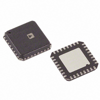
ADV7391BCPZ Analog Devices Inc, ADV7391BCPZ Datasheet - Page 7

ADV7391BCPZ
Manufacturer Part Number
ADV7391BCPZ
Description
IC ENCODER VIDEO W/DAC 32-LFCSP
Manufacturer
Analog Devices Inc
Type
Video Encoderr
Datasheet
1.ADV7393BCPZ.pdf
(108 pages)
Specifications of ADV7391BCPZ
Applications
Set-Top Boxes, Video Players, Displays
Voltage - Supply, Analog
2.6 V ~ 3.46 V
Voltage - Supply, Digital
1.71 V ~ 1.89 V
Mounting Type
Surface Mount
Package / Case
32-LFCSP
Supply Voltage Range
1.71V To 1.89V
Operating Temperature Range
-40°C To +85°C
Tv / Video Case Style
LFCSP
No. Of Pins
32
Svhc
No SVHC (18-Jun-2010)
Operating Temperature Max
85°C
Operating
RoHS Compliant
Input Format
Digital
Output Format
Analogue
Dac Resolution
10bit
Rohs Compliant
Yes
Lead Free Status / RoHS Status
Lead free / RoHS Compliant
For Use With
EVAL-ADV7391EBZ - BOARD EVAL FOR ADV7391 ENCODER
Lead Free Status / RoHS Status
Lead free / RoHS Compliant
Available stocks
Company
Part Number
Manufacturer
Quantity
Price
Company:
Part Number:
ADV7391BCPZ
Manufacturer:
CIRRUS
Quantity:
7 400
Company:
Part Number:
ADV7391BCPZ
Manufacturer:
ADI
Quantity:
302
Part Number:
ADV7391BCPZ
Manufacturer:
ADI/亚德诺
Quantity:
20 000
Company:
Part Number:
ADV7391BCPZ-3
Manufacturer:
AD
Quantity:
1 831
Company:
Part Number:
ADV7391BCPZ-REEL
Manufacturer:
HIT
Quantity:
530
Part Number:
ADV7391BCPZ-REEL
Manufacturer:
ADI/亚德诺
Quantity:
20 000
SPECIFICATIONS
POWER SUPPLY SPECIFICATIONS
All specifications T
Table 3.
Parameter
SUPPLY VOLTAGES
POWER SUPPLY REJECTION RATIO
INPUT CLOCK SPECIFICATIONS
V
All specifications T
Table 4.
Parameter
f
CLKIN High Time, t
CLKIN Low Time, t
CLKIN Peak-to-Peak Jitter Tolerance
1
ANALOG OUTPUT SPECIFICATIONS
V
All specifications T
Table 5.
Parameter
Full-Drive Output Current
Low-Drive Output Current
DAC-to-DAC Matching
Output Compliance, V
Output Capacitance, C
Analog Output Delay
DAC Analog Output Skew
1
2
CLKIN
SD = standard definition, ED = enhanced definition (525p/625p), HD = high definition.
The recommended method of bringing this value back to the ideal value is by adjusting Register 0x0B to the recommended value of 0x12.
Output delay measured from the 50% point of the rising edge of the input clock to the 50% point of the DAC output full-scale transition.
DD
DD
V
V
PV
V
DD
DD_IO
AA
= 1.71 V to 1.89 V, PV
= 1.71 V to 1.89 V, PV
DD
10
9
MIN
MIN
MIN
2
OC
OUT
to T
to T
to T
DD
DD
MAX
MAX
MAX
= 1.71 V to 1.89 V, V
= 1.71 V to 1.89 V, V
(−40°C to +85°C), unless otherwise noted.
(−40°C to +85°C), unless otherwise noted.
(−40°C to +85°C), unless otherwise noted.
Conditions
SD/ED
ED (at 54 MHz)
HD
Conditions
R
All DACs enabled
R
DAC 1 enabled only
R
DAC 1, DAC 2, DAC 3
DAC 1, DAC 2, DAC 3
SET
SET
SET
AA
AA
= 510 Ω, R
= 510 Ω, R
= 4.12 kΩ, R
= 2.6 V to 3.465 V, V
= 2.6 V to 3.465 V, V
1
Rev. B | Page 7 of 108
L
L
= 37.5 Ω
= 37.5 Ω
L
= 300 Ω
Min
40
40
1
DD_IO
DD_IO
Min
1.71
1.71
1.71
2.6
ADV7390/ADV7391/ADV7392/ADV7393
Typ
27
54
74.25
2
= 1.71 V to 3.63 V.
= 1.71 V to 3.63 V.
Typ
1.8
3.3
1.8
3.3
0.002
Max
Min
33
31.5
0
Typ
34.6
33.5
4.3
2.0
10
6
1
Unit
MHz
MHz
MHz
% of one clock cycle
% of one clock cycle
±ns
Max
1.89
3.63
1.89
3.465
Max
37
37
1.4
Unit
V
V
V
V
%/%
Unit
mA
mA
mA
%
V
pF
ns
ns


