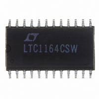
LTC1164CSW Linear Technology, LTC1164CSW Datasheet - Page 11

LTC1164CSW
Manufacturer Part Number
LTC1164CSW
Description
IC FILTER BUILDING BLOCK 24-SOIC
Manufacturer
Linear Technology
Datasheet
1.LTC1164CSWPBF.pdf
(16 pages)
Specifications of LTC1164CSW
Filter Type
Universal Switched Capacitor
Frequency - Cutoff Or Center
20kHz
Number Of Filters
4
Max-order
8th
Voltage - Supply
±2.37 V ~ 8 V
Mounting Type
Surface Mount
Package / Case
24-SOIC (7.5mm Width)
Lead Free Status / RoHS Status
Contains lead / RoHS non-compliant
Other names
LTC1164CS
Available stocks
Company
Part Number
Manufacturer
Quantity
Price
Company:
Part Number:
LTC1164CSW#PBF
Manufacturer:
Linear Technology
Quantity:
135
Part Number:
LTC1164CSW#PBF
Manufacturer:
LINEAR/凌特
Quantity:
20 000
W
Mode 3A
This is an extension of Mode 3 where the highpass and
lowpass output are summed through two external resis-
tors R
10. Mode 3A is more versatile than Mode 2 because the
notch frequency can be higher or lower than the center
frequency of the 2nd order section. The external op amp of
Figure 10 is not always required. When cascading the
sections of the LTC1164, the highpass and lowpass
V
V
IN
ODES OF OPERATIO
IN
H
R1
R1
and R
AGND
–
+
L
–
+
to create a notch. This is shown in Figure
R4
R3
R2
R4
R3
R2
Figure 10. Mode 3A: 2nd Order Filter Providing Highpass, Bandpass, Lowpass, Notch
HP
C
+
Figure 9. Mode 2: 2nd Order Filter Providing Notch, Bandpass, Lowpass
C
N
1/4 LTC1164
+
Σ
–
1/4 LTC1164
S
–
S
∫
R
H
U
BP
∫
BP
LP
R
L
LP
MODE 2 (100:1):
MODE 2 (50:1):
–
+
NOTE: THE 50:1 EQUATIONS FOR MODE 2 ARE DIFFERENT FROM THE EQUATIONS
FOR MODE 2 OPERATION OF THE LTC1059, LTC1060 AND LTC1061. START WITH
f
o
, CALCULATE R2/R4, SET R4; FROM THE Q VALUE, CALCULATE R3:
MODE 3A (100:1):
MODE 3A (50:1):
R3 =
R
G
1.005
EXTERNAL OP AMP OR
INPUT OP AMP OF THE
LTC1164, SIDE A, B, C, D
outputs can be summed directly into the inverting input of
the next section. The topology of Mode 3A is useful for
elliptic highpass and notch filters with clock to cutoff
frequency ratios higher than 100:1. This is often required
to extend the allowed input signal frequency range and to
avoid premature aliasing.
When the internal clock-to-center frequency ratio is set at
50:1, the design equations for Q and bandpass gain are
different from the 100:1 case.
Q
f
H
f
H
R2
H
o
o
1 +
NOTCH
OBP
OBP
ON2
=
=
NOTE: THE 50:1 EQUATIONS FOR MODE 3A ARE DIFFERENT FROM THE EQUATIONS
FOR MODE 3A OPERATION OF THE LTC1059, LTC1060 AND LTC1061. START WITH
f
o
, CALCULATE R2/R4, SET R4; FROM THE Q VALUE, CALCULATE R3:
f
f
100
CLK
CLK
R2
R4
50
R3 =
= –
= –
H
H
H
f
f
o
o
f
OLP
ON
OBP
=
=
+
R3/R1;
1 – (R3/16R4)
16R4
f
100
f
(f = f
CLK
CLK
50
1.005
f
R2
= –
= –
CLK
2
1 +
1 +
Q
R3/R1
R4/R1;
o
1 – (R3/16R4)
H
) = Q
R2
R4
R2
R4
; THEN CALCULATE R1 TO SET THE DESIRED GAIN
ON1
= – R2/R1
R2
R2
R4
R2
R4
R3/R1
; f
; f
R2
R4
(f
H
(
n
n
; f
R
; f
R
; H
ON1
=
=
G
L
n
n
+
f
f
H
ON1
16R4
=
=
CLK
50
CLK
50
0) =
(f → 0) =
OLP
R2
f
f
100
CLK
CLK
50
(f
; H
; Q =
; Q =
–
1 + (R2/R4)
; THEN CALCULATE R1 TO SET
OLP
R
R
THE DESIRED GAIN
– R2/R1
0) =
G
H
(R2/R3) – (R2/16R4)
(f = 0) = – R4/R1
R3
R2
1.005 ( 1 + R2/R4)
R
R
H
R
R
R
R
H
OHP
H
L
G
L
L
1 + (R2/R4)
; H
; H
×
– R2/R1
)
1 + R2
OHP
OHP
; Q =
R4
R1
; H
; H
R4
ON2
= – R2/R1; H
(
R3
R2
f →
ON2
; H
f
f
OLP
; Q =
(
CLK
2
f →
R2
R4
=
f
)
; H
CLK
(R2/R3) – (R2/16R4)
2
f
= –R2/R1
LTC1164
1 + (R2/R4)
CLK
OLP
OBP
2
1.005 (√R2/R4)
–R2/R1
)
= – R2/R1
=
= –R3/R1
=
1 + (R2/R4)
R
R
LTC1164 • MOO05
– R2/R1
G
H
×
R2
R1
LTC1164 • MOO04
11
1164fa


