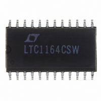
LTC1164CSW Linear Technology, LTC1164CSW Datasheet - Page 9

LTC1164CSW
Manufacturer Part Number
LTC1164CSW
Description
IC FILTER BUILDING BLOCK 24-SOIC
Manufacturer
Linear Technology
Datasheet
1.LTC1164CSWPBF.pdf
(16 pages)
Specifications of LTC1164CSW
Filter Type
Universal Switched Capacitor
Frequency - Cutoff Or Center
20kHz
Number Of Filters
4
Max-order
8th
Voltage - Supply
±2.37 V ~ 8 V
Mounting Type
Surface Mount
Package / Case
24-SOIC (7.5mm Width)
Lead Free Status / RoHS Status
Contains lead / RoHS non-compliant
Other names
LTC1164CS
Available stocks
Company
Part Number
Manufacturer
Quantity
Price
Company:
Part Number:
LTC1164CSW#PBF
Manufacturer:
Linear Technology
Quantity:
135
Part Number:
LTC1164CSW#PBF
Manufacturer:
LINEAR/凌特
Quantity:
20 000
W
APPLICATIO S I FOR ATIO
3. Offset Nulling
Lowpass filters may have too much DC offset for some
users. A servo circuit may be used to actively null the
offsets of the LTC1164 or any LTC switched capacitor
filter. The circuit shown in Figure 5 will null offsets to better
than 300µV. This circuit takes seconds to settle because of
the integrator pole frequency.
PRIMARY MODES
Mode 1
In Mode 1, the ratio of the external clock frequency to the
center frequency of each 2nd order section is internally
fixed at 50:1 or 100:1. Figure 6 illustrates Mode 1 provid-
ing 2nd order notch, lowpass, and bandpass outputs.
Mode 1 can be used to make high order Butterworth
Iowpass filters; it can also be used to make low Q notches
and for cascading 2nd order bandpass functions tuned at
the same center frequency with unity gain. Mode 1 is faster
than Mode 3. Note that Mode 1 can only be implemented
with 3 of the 4 LTC1164 sections because section D has no
externally available summing node. Section D, however,
can be internally connected in Mode 1 upon special
request.
V
Figure 4. Buffering the Output of a 4th Order Bandpass Realization
+
V
TRACE FOR FILTER
ODES OF OPERATIO
IN
POSITIVE
SUPPLY
R11
0.1µF
SEPARATE V
R21
R3
+
POWER SUPPLY TRACE FOR BUFFER
U
7
LTC1164
U
19
W
R12
R22
R32
1k
U
NEGATIVE
0.1µF
SUPPLY
–
+
U
4
7
1µF T
1µF T
A
LTC1164 • AI02
A
4. Noise
All the noise performance mentioned excludes the clock
feedthrough. Noise measurements will degrade if the
already described grounding, bypassing, and buffering
techniques are not practiced. The Wideband Noise vs Q
curve shown in the Typical Performance Characteristics
Section is a very good representation of the noise
performance of this device.
0.1µF
0.1µF
V
IN
Figure 6. Mode 1: 2nd Order Filter Providing Notch,
Bandpass, Lowpass
R1
FIRST SUMMING
C1 = C2 = LOW LEAKAGE FILM (I.E. POLYPROPYLENE)
R1 = R2 = METAL FILM 1%
f
o
=
TO FILTER
100(50)
NODE
f
AGND
CLK
–
+
; f
Figure 5. Servo Amplifier
R3
R2
n
= f
O
; H
100k
R3
OLP
= –
N
1/4 LTC1164
R2
R1
+
; H
OBP
0.1µF
–
LT1012
C2
S
= –
+
–
R3
R1
; H
ON1
LTC1164
FROM
FILTER
OUTPUT
BP
R2
1M
= –
R1
1M
LTC1164 • AI03
R2
R1
C1
0.1µF
LTC1164 • MOO01
Q =
LP
R3
R2
1164fa
9


