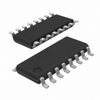
SI2493-C-FS Silicon Laboratories Inc, SI2493-C-FS Datasheet - Page 152

SI2493-C-FS
Manufacturer Part Number
SI2493-C-FS
Description
IC ISOMODEM SYSTEM-SIDE 16SOIC
Manufacturer
Silicon Laboratories Inc
Specifications of SI2493-C-FS
Mfg Application Notes
SI2493/57/34/15/04, Appl Note AN93
Data Format
V.21, V.22, V.23, V.29, V.32, V.34, V.90, V.92, Bell 103, Bell 212A
Baud Rates
56k
Interface
UART
Voltage - Supply
3 V ~ 3.6 V
Mounting Type
Surface Mount
Package / Case
16-SOIC (3.9mm Width)
Lead Free Status / RoHS Status
Lead free / RoHS Compliant
Available stocks
Company
Part Number
Manufacturer
Quantity
Price
Company:
Part Number:
SI2493-C-FSR
Manufacturer:
DY
Quantity:
8 623
Part Number:
SI2493-C-FSR
Manufacturer:
SIEMENS/西门子
Quantity:
20 000
- Current page: 152 of 230
- Download datasheet (7Mb)
AN93
9. U2 pin 15 is also known as IGND. This is the ground
152
return path for many of the discrete components and
requires special mention:
a.Space U2, Q4, Q5, R1, R3, R4, R10 and R11
b.The tightest layout can be achieved by grouping
c.Place C3 next to D1.
d.Make the size of the Q3, Q4, and Q5 collector
a.Route traces associated with IGND using 20 mil
away from each other for best thermal
performance.
R6, C10, Q2, R3, R5, and Q1.
pads each sufficiently large for the transistor to
safely dissipate 0.5 W under worst case
conditions. See the transistor data sheet for
thermal resistance and maximum operating
temperature information. Implement collector
pads on both the component and solder side, and
use vias between them to improve heat transfer
for best performance.
traces.
Figure 27. Reference Placement
Rev. 0.9
10.The traces from R7 to FB1 and from R8 to FB2
11. Minimize all traces associated with Y1, C40, and
12.Decoupling capacitors (size 0.22 µF and 0.1 µF
should be well matched. This can be achieved by
routing these traces next to each other as possible.
Ensure that these traces are not routed close to the
traces connected to C1 or C2.
C41.
capacitors connected to V
placed next to those pins. Traces of these
decoupling capacitors back to the Si24xx GND pin
should be direct and short.
b.The area underneath U2 should be ground-filled
c.C5, C6, C7 IGND return path should be direct.
d.The IGND plane must not extend past Q4 and
and connected to IGND (U2 pin 15). Ground fill
both the solder side and the component side and
stitch together using vias.
Q5.
DA
, V
DB
, V
DD
) must be
Related parts for SI2493-C-FS
Image
Part Number
Description
Manufacturer
Datasheet
Request
R
Part Number:
Description:
SOIC 16/C�/56 KBPS, V.92 ISOMODEM 16-PIN SYSTEM-SIDE - LEAD-FREE
Manufacturer:
Silicon Laboratories Inc
Part Number:
Description:
TSSOP 24/I�/56 KBPS, V.92 ISOMODEM SYSTEM-SIDE
Manufacturer:
Silicon Laboratories Inc
Part Number:
Description:
IC ISOMODEM SYSTEM-SIDE 24TSSOP
Manufacturer:
Silicon Laboratories Inc
Datasheet:
Part Number:
Description:
56 KBPS, V.92 ISOMODEM SYSTEM-SIDE - LEAD-FREE TSSOP 0 TO 7
Manufacturer:
Silicon Laboratories Inc
Datasheet:
Part Number:
Description:
Telecom ICs CONTACT SILICON LABS FOR AVAILABILITY
Manufacturer:
Silicon Laboratories Inc
Part Number:
Description:
IC ISOMODEM SYSTEM-SIDE 16SOIC
Manufacturer:
Silicon Laboratories Inc
Datasheet:
Part Number:
Description:
IC ISOMODEM SYSTEM-SIDE 24TSSOP
Manufacturer:
Silicon Laboratories Inc
Datasheet:

Part Number:
Description:
IC ISOMODEM W/ERROR CORR 16SOIC
Manufacturer:
Silicon Laboratories Inc
Datasheet:
Part Number:
Description:
IC ISOMODEM W/ERROR CORR 24TSSOP
Manufacturer:
Silicon Laboratories Inc
Datasheet:

Part Number:
Description:
IC ISOMODEM W/DAA 16SOIC
Manufacturer:
Silicon Laboratories Inc
Datasheet:
Part Number:
Description:
IC ISOMODEM SYSTEM-SIDE 24TSSOP
Manufacturer:
Silicon Laboratories Inc
Datasheet:
Part Number:
Description:
IC ISOMODEM W/ERROR CORR 24TSSOP
Manufacturer:
Silicon Laboratories Inc
Datasheet:
Part Number:
Description:
IC ISOMODEM W/DAA 24TSSOP
Manufacturer:
Silicon Laboratories Inc
Datasheet:


