AD693AQ Analog Devices Inc, AD693AQ Datasheet - Page 3
AD693AQ
Manufacturer Part Number
AD693AQ
Description
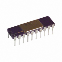
IC TRANSMITTER 4-20MA 20-CDIP
Manufacturer
Analog Devices Inc
Type
Signal Conditionerr
Datasheet
1.AD693AQ.pdf
(12 pages)
Specifications of AD693AQ
Rohs Status
RoHS non-compliant
Input Type
Voltage
Output Type
Voltage
Interface
3-Wire
Current - Supply
20mA
Mounting Type
Through Hole
Package / Case
20-CDIP (0.300", 7.62mm)
Supply Voltage Range
12V To 36V
Operating Temperature Range
-40°C To +85°C
Digital Ic Case Style
DIP
No. Of Pins
20
Svhc
No SVHC (18-Jun-2010)
Operating Temperature Max
85°C
Operating
RoHS Compliant
Converter Type
Voltage to Current
Current, Output
+25 mA (Typ.)
Current, Quiescent Supply
+500 uA (Typ.)
Package Type
Cerdip
Temperature, Operating, Maximum
85 °C
Temperature, Operating, Minimum
-40 °C
Voltage, Operating
+12 V (Min.)
No. Of Amplifiers
5
Input Offset Voltage
200µV
Cmrr
90dB
Supply Current
500µA
Amplifier Case Style
DIP
Rohs Compliant
No
Ic Function
Sensor Transmitter
Amplifier Type
Current
Base Number
693
Lead Free Status / RoHS Status
Available stocks
Company
Part Number
Manufacturer
Quantity
Price
Company:

Part Number:
AD693AQ
Manufacturer:
TOSHIBA
Quantity:
101
Part Number:
AD693AQ
Manufacturer:
ADI/亚德诺
Quantity:
20 000


NOTES
10
11
12
13
14
Specifications subject to change without notice.
Specifications shown in boldface are tested on all production units at final electrical test. Results from those tests are used to calculate outgoing quality levels. All min
and max specifications are guaranteed, although only those shown in boldface are tested on all production units.
ABSOLUTE MAXIMUM RATINGS
Supply Voltage . . . . . . . . . . . . . . . . . . . . . . . . . . . . . . . . +36 V
Reverse Loop Current . . . . . . . . . . . . . . . . . . . . . . . . . 200 mA
Signal Amp Input Range . . . . . . . . . . . . . . . . . . –0.3 V to V
Reference Short Circuit to Common . . . . . . . . . . . . Indefinite
Auxiliary Amp Input Voltage Range . . . . . . . . . . 0.3 V to V
Auxiliary Amp Current Output . . . . . . . . . . . . . . . . . . . 10 mA
Storage Temperature . . . . . . . . . . . . . . . . . . –65 C to +150 C
Lead Temperature, 10 sec Soldering . . . . . . . . . . . . . +300 C
Max Junction Temperature . . . . . . . . . . . . . . . . . . . . . +150 C
Model
AD693AD
AD693AQ
AD693AE
REV. A
1
2
3
4
5
6
7
8
9
Bias currents are not symmetrical with input signal level and flow out of the input pins. The input bias current of the inverting input increases with input signal volt-
Total error can be significantly reduced (typically less than 0.1%) by trimming the zero current. The remaining unadjusted error sources are transconductance and
nonlinearity.
The AD693 is tested as a loop powered device with the signal amp, V/I converter, voltage reference, and application voltages operating together. Specifications are
valid for preset spans and spans between 30 mV and 60 mV.
Error from ideal output assuming a perfect 100
Refer to the Error Analysis to calculate zero current error for input spans less than 30 mV.
By forcing the differential signal amplifier input sufficiently negative the 7 A zero current can always be achieved.
The operational voltage (V
(I
age, see Figure 2.
Nonlinearity is defined as the deviation of the output from a straight line connecting the endpoints as the input is swept over a 30 mV and 60 mV input span.
Specifications for the individual functional blocks are components of error that contribute to, and that are included in, the Loop Powered Operation specifications.
Includes error contributions of V/I converter and Application Voltages.
Changes in the reference output voltage due to load will affect the Zero Current. A 1% change in the voltage reference output will result in an error of 1% in the
value of the Zero Current.
If not used for external excitation, the reference should be loaded by approximately 1 mA (6.2 k to common).
In the loop powered mode up to 5 mA can be drawn from the reference, however, the lower limit of the output span will be increased accordingly. 3.5 mA is the
maximum current the reference can source while still maintaining a 4 mA zero.
The AD693 is tested with a pass transistor so T
Model
AUXILIARY AMPLIFIER
TEMPERATURE RANGE
LOOP
Common-Mode Range
Input Offset Voltage
Input Bias Current
Input Offset Current
Common-Mode Rejection
Power Supply Rejection
Output Current Range
Output Current Error
Case Operating
Storage
R
L
) in two-wire mode (refer to Figure 10).
Package
Description
Ceramic Side-Brazed DIP
Cerdip
Leadless Ceramic Chip
Carrier (LCCC)
14
ORDERING GUIDE
OP
) is the voltage directly across the AD693 (Pin 10 to 6 in two-wire mode, Pin 9 to 6 in local power mode). For example, V
A
RTD at 0 and +100 C.
T
C
.
Conditions
Pin I
Pin V
T
MIN
Package
Option
D-20
Q-20
E-20A
X
X
to T
OUT
– Pin I
MAX
OP
OP
X
–3–
Min
0
+0.01
–40
–65
AD693 PIN CONFIGURATION
AD693AD
(AD, AQ, AE Packages)
Functional Diagram
Typ
+5
+0.5
90
105
50
0.005
Max
+V
+20
+5
+85
+150
200
3.0
OP
– 4 V
6
Units
V
nA
dB
dB
mA
%
nA
C
C
V
OP
AD693
= V
S
–
Related parts for AD693AQ
Image
Part Number
Description
Manufacturer
Datasheet
Request
R

Part Number:
Description:
±1.7g Dual-Axis IMEMS Accelerometer Evaluation Board
Manufacturer:
Analog Devices Inc
Datasheet:

Part Number:
Description:
Inertial Sensor Evaluation System
Manufacturer:
Analog Devices Inc
Datasheet:
Part Number:
Description:
Manufacturer:
Analog Devices Inc
Datasheet:
Part Number:
Description:
Manufacturer:
Analog Devices Inc
Datasheet:
Part Number:
Description:
Manufacturer:
Analog Devices Inc
Datasheet:
Part Number:
Description:
Manufacturer:
Analog Devices Inc
Datasheet:
Part Number:
Description:
Manufacturer:
Analog Devices Inc
Datasheet:
Part Number:
Description:
Manufacturer:
Analog Devices Inc
Datasheet:
Part Number:
Description:
Manufacturer:
Analog Devices Inc
Datasheet:
Part Number:
Description:
Manufacturer:
Analog Devices Inc
Datasheet:
Part Number:
Description:
Manufacturer:
Analog Devices Inc
Datasheet:
Part Number:
Description:
Manufacturer:
Analog Devices Inc
Datasheet:
Part Number:
Description:
Manufacturer:
Analog Devices Inc
Datasheet: